Application Information: continued
where
PGATE(H) = upper MOSFET gate driver (IC) losses;
caused by sudden and fast load changes. These load tran-
sients can have slew rates as high as 20A/µs.
QGATE(H) = total upper MOSFET gate charge;
FSW = switching frequency;
“Droop” Resistor for Adaptive Voltage Positioning
and Current Limit
VGATE(H) = upper MOSFET gate voltage.
The lower (synchronous) MOSFET gate driver (IC) losses
are:
Adaptive voltage positioning is used to help keep the out-
put voltage within specification during load transients. To
implement adaptive voltage positioning a “Droop
PGATE(L) = QGATE(L) × FSW × VGATE(L)
,
Resistor” must be connected between the output inductor
and output capacitors and load. This resistor carries the
full load current and should be chosen so that both DC and
AC tolerance limits are met. An embedded PC trace resis-
tor has the distinct advantage of near zero cost implemen-
tation. However, this droop resistor can vary due to three
reasons: 1) the sheet resistivity variation caused by varia-
tion in the thickness of the PCB layer; 2) the mismatch of
L/W; and 3) temperature variation.
where
PGATE(L) = lower MOSFET gate driver (IC) losses;
QGATE(L) = total lower MOSFET gate charge;
FSW = switching frequency;
VGATE(L) = lower MOSFET gate voltage.
The junction temperature of the control IC is primarily a
function of the PCB layout, since most of the heat is
removed through the traces connected to the pins of the
IC.
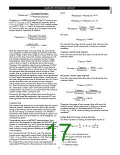
1) Sheet Resistivity
Step 9: Slope Compensation
For one ounce copper, the thickness variation is typically
1.26 mil to 1.48 mil. Therefore the error due to sheet resis-
tivity is:
Voltage regulators for today’s advanced processors are
expected to meet very stringent load transient require-
ments. One of the key factors in achieving tight dynamic
voltage regulation is low ESR at the CPU input supply
pins. Low ESR at the regulator output results in low out-
put voltage ripple. The consequence is, however, that
there’s very little voltage ramp at the control IC feedback
pin (VFB) and regulator sensitivity to noise and loop insta-
bility are two undesirable effects that can surface. The per-
formance of the CS51313-based CPU VCC(CORE) regulator is
improved when a fixed amount of slope compensation is
added to the output of the PWM Error Amplifier (COMP
pin) during the regulator Off-Time. Referring to Figure 12,
the amount of voltage ramp at the COMP pin is dependent
on the gate voltage of the lower (synchronous) FET and the
value of resistor divider formed by R1and R2.
1.48 - 1.26
= ±8%.
1.37
2) Mismatch due to L/W
The variation in L/W is governed by variations due to the
PCB manufacturing process. The error due to L/W mis-
match is typically 1%.
3) Thermal Considerations
Due to I2 × R power losses the surface temperature of the
droop resistor will increase causing the resistance to
increase. Also, the ambient temperature variation will con-
tribute to the increase of the resistance, according to the
formula:
R = R20 [1+ α20(Τ−20)],
-t
R2
R1 + R2
VSLOPECOMP = VGATE(L)
×
× (1 − eτ ),
(
)
where
where
R20 = resistance at 20˚C;
VSLOPECOMP = amount of slope added;
GATE(L) = lower MOSFET gate voltage;
R1, R2 = voltage divider resistors;
t = tOFF (switch off-time);
τ = RC constant determined by C1 and the parallel com-
bination of R1, R2 (Figure 12), neglecting the low driver
output impedance
0.00393
V
α =
;
˚C
T= operating temperature;
R = desired droop resistor value.
For temperature T = 50˚C, the % R change = 12%.
The artificial voltage ramp created by the slope compensa-
tion scheme results in improved control loop stability pro-
vided that the RC filter time constant is smaller than the
off-time cycle duration (time during which the lower MOS-
FET is conducting).
Droop Resistor Tolerance
Tolerance due to sheet resistivity variation
Tolerance due to L/W error
Tolerance due to temperature variation
Total tolerance for droop resistor
±8%
1%
12%
21%
Step 10: Selection of Current Limit Filter Components
In order to determine the droop resistor value the nominal
voltage drop across it at full load has to be calculated. This
voltage drop has to be such that the output voltage at full
load is above the minimum DC tolerance spec:
The current limit filter is implemented by a 0.1µF ceramic
capacitor across and two 510Ω resistors in series with the
V
FB and VOUT current limit comparator input pins. They
provide a time constant τ = RC = 100µs, which enables the
circuit to filter out noise and be immune to false triggering,
16

 CHERRY [ CHERRY SEMICONDUCTOR CORPORATION ]