Application Information: continued
filter and bypass capacitors, as well as other loads located
7) The MOSFET gate traces to the IC must be as short,
straight, and wide as possible.
on the board will tend to reduce regulator di/dt effects on
the circuit board and input power supply. Placement of the
power component to minimize routing distance will also
help to reduce emissions.
8) Use fewer, but larger output capacitors, keep the capaci-
tors clustered, and use multiple layer traces with heavy
copper to keep the parasitic resistance low.
9) Place the switching MOSFET as close to the +5V input
capacitors as possible.
Layout Guidelines
When laying out the CPU buck regulator on a printed cir-
cuit board, the following checklist should be used to
ensure proper operation of the CS51312.
10) Place the output capacitors as close to the load as possi-
ble.
11) Place the VFB,VOUT filter resistors (510Ω) in series with
the VFB and VOUT pins as close as possible to the pins.
1) Rapid changes in voltage across parasitic capacitors and
abrupt changes in current in parasitic inductors are major
concerns for a good layout.
12) Place the COFF and COMP capacitors as close as possi-
ble to the COFF and COMP pins.
2) Keep high currents out of sensitive ground connections.
13) Place the current limit filter capacitor between the VFB
and VOUT pins, as close as possible to the pins.
3) Avoid ground loops as they pick up noise. Use star or
single point grounding.
14) Connect the filter components of the following pins:
4) For high power buck regulators on double-sided PCBs a VFB, VOUT, COFF, and COMP to the Gnd pin with a single
single ground plane (usually the bottom) is recommended. trace, and connect this local Gnd trace to the output capaci-
tor Gnd.
5) Even though double sided PCBs are usually sufficient
for a good layout, four-layer PCBs are the optimum
approach to reducing susceptibility to noise. Use the two
internal layers as the power and Gnd planes, the top layer
for power connections and components vias, and the bot-
tom layers for the noise sensitive traces.
15) The “Droop” Resistor (embedded PCB trace) has to be
wide enough to carry the full load current.
16) Place the VCC bypass capacitors as close as possible to
the IC.
6) Keep the inductor switching node small by placing the
output inductor, switching and synchronous FETs close
together.
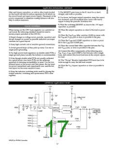
Additional Application Circuit
+5V
+12V
1µF
1200µF/10V
680pF
x3
10K
FS70VSJ-03
FS70VSJ-03
0.01
µF
0.1
µF
1.2µH
3.3mΩ
100Ω
COFF VCC1
COMP
VCC2
GATE(H)
GATE(L)
VCC(CORE)
2.0V@19A
1200µF/10V
x5
VID0
VFB
VID1
VID2
VID3
VID4
510Ω
VOUT
OVP
0.1µF
Gnd
PWRGD
510Ω
OVP
PWRGD
5V/12V to 2V/19A Converter
17

 CHERRY [ CHERRY SEMICONDUCTOR CORPORATION ]