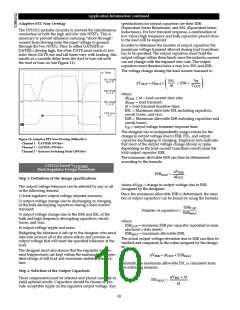
Application Information: continued
specifications for output capacitors are their ESR
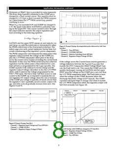
Adaptive FET Non-Overlap
(Equivalent Series Resistance), and ESL (Equivalent Series
Inductance). For best transient response, a combination of
low value/high frequency and bulk capacitors placed close
to the load will be required.
In order to determine the number of output capacitors the
maximum voltage transient allowed during load transitions
has to be specified. The output capacitors must hold the
output voltage within these limits since the inductor current
can not change with the required slew rate. The output
capacitors must therefore have a very low ESL and ESR.
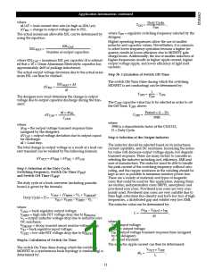
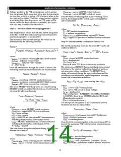
The CS51312 includes circuitry to prevent the simultaneous
conduction of both the high and low side NFETs. This is
necessary to prevent efficiency reducing “shoot-through”
current from flowing from the input voltage to ground
through the two NFETs. Prior to either GATE(H) or
GATE(L) driving high, the other GATE must reach its low
state. Since GATE rise and fall times vary with loading, this
results in a variable delay from the start of turn-off until
the start of turn-on (see Figure 11).
The voltage change during the load current transient is:
tTR
COUT
ESL
∆t
∆VOUT = ∆IOUT
×
+ ESR +
,
(
)
where
∆IOUT / ∆t = load current slew rate;
∆IOUT = load transient;
∆t = load transient duration time;
ESL = Maximum allowable ESL including capacitors,
circuit traces, and vias;
ESR = Maximum allowable ESR including capacitors and
circuit traces;
tTR = output voltage transient response time.
The designer has to independently assign values for the
change in output voltage due to ESR, ESL, and output
capacitor discharging or charging. Empirical data indicates
that most of the output voltage change (droop or spike
depending on the load current transition) results from the
total output capacitor ESR.
Figure 11: Adaptive FET Non-Overlap (100ns/div).
Channel 1 - GATE(H) (5V/div)
Channel 2 – GATE(L) (5V/div)
Channel 3 - Inductor Switching Node (10V/div)
The maximum allowable ESR can then be determined
according to the formula
CS51312-based VCC(CORE)
Buck Regulator Design Procedure
∆VESR
ESRMAX
=
,
∆IOUT
Step 1: Definition of the design specifications
where ∆VESR = change in output voltage due to ESR
The output voltage tolerance can be affected by any or all
of the following reasons:
1) buck regulator output voltage setpoint accuracy;
2) output voltage change due to discharging or charging
of the bulk decoupling capacitors during a load current
transient;
3) output voltage change due to the ESR and ESL of the
bulk and high frequency decoupling capacitors, circuit
traces, and vias;
(assigned by the designer).
Once the maximum allowable ESR is determined, the num-
ber of output capacitors can be found by using the formula
ESRCAP
ESRMAX
Number of capacitors =
,
where
ESRCAP = maximum ESR per capacitor (specified in man-
ufacturer’s data sheet);
4) output voltage ripple and noise.
Budgeting the tolerance is left up to the designer who must
take into account all of the above effects and provide an
output voltage that will meet the specified tolerance at the
load.
The designer must also ensure that the regulator compo-
nent temperatures are kept within the manufacturer’s spec-
ified ratings at full load and maximum ambient tempera-
ture.
ESRMAX = maximum allowable ESR.
The actual output voltage deviation due to ESR can then be
verified and compared to the value assigned by the design-
er:
∆VESR = ∆IOUT × ESRMAX
Similarly, the maximum allowable ESL is calculated from
the following formula:
Step 2: Selection of the Output Capacitors
∆VESL × ∆t
These components must be selected and placed carefully to
yield optimal results. Capacitors should be chosen to pro-
vide acceptable ripple on the regulator output voltage. Key
ESLMAX
=
,
∆I
10

 CHERRY [ CHERRY SEMICONDUCTOR CORPORATION ]