Application Information: continued
where
Duty Cycle
FSW
TON
=
,
∆I/∆T = load current slew rate (as high as 20A/µs);
∆VESL = change in output voltage due to ESL.
where FSW = regulator switching frequency selected by the
designer.
The actual maximum allowable ESL can be determined by
using the equation:
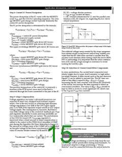
Higher operating frequencies allow the use of smaller
inductor and capacitor values. Nevertheless, it is common
to select lower frequency operation because a higher fre-
quency results in lower efficiency due to MOSFET gate
charge losses. Additionally, the use of smaller inductors at
higher frequencies results in higher ripple current, higher
output voltage ripple, and lower efficiency at light load
currents.
ESLCAP
ESLMAX
=
,
Number of output capacitors
where ESLCAP = maximum ESL per capacitor (it is estimat-
ed that a 10 × 12mm Aluminum Electrolytic capacitor has
approximately 4nH of package inductance).
The actual output voltage deviation due to the actual maxi-
mum ESL can then be verified:
Step 3b: Calculation of Switch Off-Time
The switch Off-Time (time during which the switching
MOSFET is not conducting) can be determined by:
ESLMAX × ∆I
∆VESL
=
.
∆t
1
FSW
TOFF
=
− TON,
The designer now must determine the change in output
voltage due to output capacitor discharge during the tran-
sient:
The COFF capacitor value has to be selected in order to set
the Off-Time, TOFF, above:
Period × (1 − D)
∆I × ∆tTR
COFF
=
,
∆VCAP
=
,
3980
COUT
where
where
3980 is a characteristic factor of the CS51312;
D = Duty Cycle.
∆tTR = the output voltage transient response time
(assigned by the designer);
∆VCAP = output voltage deviation due to output capaci-
tor discharge;
∆I = Load step.
Step 4: Selection of the Output Inductor
The inductor should be selected based on its inductance,
current capability, and DC resistance. Increasing the induc-
tor value will decrease output voltage ripple, but degrade
transient response. There are many factors to consider in
selecting the inductor including cost, efficiency, EMI and
ease of manufacture. The inductor must be able to handle
the peak current at the switching frequency without satu-
rating, and the copper resistance in the winding should be
kept as low as possible to minimize resistive power loss.
There are a variety of materials and types of magnetic
cores that could be used for this application. Among them
are ferrites, molypermalloy cores (MPP), amorphous and
powdered iron cores. Powdered iron cores are very com-
monly used. Powdered iron cores are very suitable due to
their high saturation flux density and have low loss at high
frequencies, a distributed gap and exhibit very low EMI.
The total change in output voltage as a result of a load cur-
rent transient can be verified by the following formula:
∆VOUT = ∆VESR + ∆VESL + ∆VCAP
Step 3: Selection of the Duty Cycle,
Switching Frequency, Switch On-Time (TON
)
and Switch Off-Time (TOFF
)
The duty cycle of a buck converter (including parasitic
losses) is given by the formula:
VOUT + (VHFET + VL + VDROOP
)
Duty Cycle = D =
,
VIN + VLFET − VHFET − VL
The inductor value can be determined by:
where
VOUT = buck regulator output voltage;
HFET = high side FET voltage drop due to RDS(ON)
VL = output inductor voltage drop due to inductor wire
DC resistance;
(VIN − VOUT) × tTR
L =
,
V
;
∆Ι
where
VIN = input voltage;
V
DROOP = droop (current sense) resistor voltage drop;
VIN = buck regulator input voltage;
LFET = low side FET voltage drop due to RDS(ON)
VOUT = output voltage;
t
TR = output voltage transient response time (assigned
V
.
by the designer);
∆I = load transient.
Step3a: Calculation of Switch On-Time
The inductor ripple current can then be determined:
The switch On-Time (time during which the switching
MOSFET in a synchronous buck topology is conducting) is
determined by:
VOUT × TOFF
∆IL =
,
L
11

 CHERRY [ CHERRY SEMICONDUCTOR CORPORATION ]