Application Information: continued
and output capacitors and load. This resistor carries the
full load current and should be chosen so that both DC and
AC tolerance limits are met.
In order to determine the droop resistor value the nominal
voltage drop across it at full load has to be calculated. This
voltage drop has to be such that the output voltage at full
load is above the minimum DC tolerance spec:
3) Thermal Considerations
Due to I2 × R power losses the surface temperature of the
droop resistor will increase causing the resistance to
increase. Also, the ambient temperature variation will con-
tribute to the increase of the resistance, according to the
formula:
R = R20 [1+ α20(Τ−20)],
where
VDAC(MIN)-VDC(MIN)
VDROOP(TYP)
=
.
R
20 = resistance at 20˚C;
1+RDROOP(TOLERANCE)
0.00393
α =
;
˚C
Current Limit
T= operating temperature;
R = desired droop resistor value.
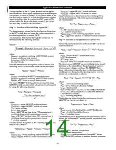
For temperature T = 50˚C, the % R change = 12%.
The current limit setpoint has to be higher than the normal
full load current. Attention has to be paid to the current
rating of the external power components as these are the
first to fail during an overload condition. The MOSFET
continuous and pulsed drain current rating at a given case
temperature has to be accounted for when setting the cur-
rent limit trip point.
Droop Resistor Tolerance
Tolerance due to sheet resistivity variation
Tolerance due to L/W error
Tolerance due to temperature variation
Total tolerance for droop resistor
±8%
1%
12%
21%
Nominal Current Limit Setpoint
From the overcurrent detection data in the electrical char-
acteristics table:
Droop Resistor Length, Width, and Thickness
VTH(TYP) = 86mV,
VTH(TYP)
The minimum width and thickness of the droop resistor
should primarily be determined on the basis of the current-
carrying capacity required, and the maximum permissible
droop resistor temperature rise. PCB manufacturer design
charts can be used in determining current- carrying capaci-
ty and sizes of etched copper conductors for various tem-
perature rises above ambient.
ICL(NOM)
=
RSENSE(NOM)
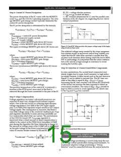
Design Rules for Using a Droop Resistor
The basic equation for laying an embedded resistor is:
Thermal Management
L
L
R
AR = ρ ×
or R = ρ ×
,
A
(W × t)
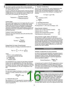
Thermal Considerations for Power MOSFET
In order to maintain good reliability, the junction tempera-
ture of the semiconductor components should be kept to a
maximum of 150°C or lower. The thermal impedance
(junction to ambient) required to meet this requirement
can be calculated as follows:
where
A= W × t = cross-sectional area;
ρ= the copper resistivity (µΩ-mil);
L= length (mils);
W = width (mils);
t = thickness (mils).
T
J(MAX) - TA
Thermal Impedance =
Power
An embedded PC trace resistor has the distinct advantage
of near zero cost implementation. However, this droop
resistor can vary due to three reasons: 1) the sheet resistivi-
ty variation caused by variation in the thickness of the PCB
layer; 2) the mismatch of L/W; and 3) temperature varia-
tion.
A heatsink may be added to TO-220 components to reduce
their thermal impedance. A number of PC board layout
techniques such as thermal vias and additional copper foil
area can be used to improve the power handling capability
of surface mount components.
1) Sheet Resistivity
For one ounce copper, the thickness variation is typically
1.26 mil to 1.48 mil. Therefore the error due to sheet resis-
tivity is:
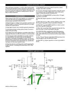
EMI Management
As a consequence of large currents being turned on and off
at high frequency, switching regulators generate noise as a
consequence of their normal operation. When designing
for compliance with EMI/EMC regulations, additional
components may be added to reduce noise emissions.
These components are not required for regulator operation
and experimental results may allow them to be eliminated.
The input filter inductor may not be required because bulk
1.48 - 1.26
= ±8%.
1.37
2) Mismatch due to L/W
The variation in L/W is governed by variations due to the
PCB manufacturing process. The error due to L/W mis-
match is typically 1%.
16

 CHERRY [ CHERRY SEMICONDUCTOR CORPORATION ]