Application Information: continued
Step 8: Control IC Power Dissipation
R1, R2 = voltage divider resistors;
t = tON or tOFF (switch off-time);
The power dissipation of the IC varies with the MOSFETs
used, VCC, and the CS51312 operating frequency. The aver-
age MOSFET gate charge current typically dominates the
control IC power dissipation.
τ = RC constant determined by C1 and the parallel com-
bination of R1, R2 (Figure 12), neglecting the low driver
output impedance.
The IC power dissipation is determined by the formula:
16
COMP
C
2
COMP
PCONTROLIC = ICC1VCC1 + PGATE(H) + PGATE(L)
,
CS51312
GATE(L)
where
CONTROLIC = control IC power dissipation;
ICC1 = IC quiescent supply current;
VCC1 = IC supply voltage;
R
C
R
1
1
P
12
To Synchronous FET
PGATE(H) = upper MOSFET gate driver (IC) losses;
PGATE(L) = lower MOSFET gate driver (IC) losses.
The upper (switching) MOSFET gate driver (IC) losses are:
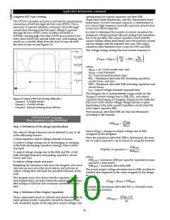
Figure 12: Small RC filter provides the proper voltage ramp at the begin-
ning of each on-time cycle.
P
GATE(H) = QGATE(H) × FSW × VGATE(H),
The artificial voltage ramp created by the slope compensa-
tion scheme results in improved control loop stability pro-
vided that the RC filter time constant is smaller than the
off-time cycle duration (time during which the lower MOS-
FET is conducting). It is important that the series combina-
tion of R1 and R2 is high enough in resistance to avoid
loading the GATE(L) pin.
where
PGATE(H) = upper MOSFET gate driver (IC) losses;
QGATE(H) = total upper MOSFET gate charge;
SW = switching frequency;
VGATE(H) = upper MOSFET gate voltage.
F
The lower (synchronous) MOSFET gate driver (IC) losses
are:
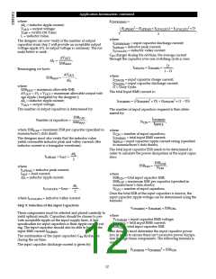
Step 10: Selection of Current Limit Filter Components
In some applications, the current limit comparator may
falsely trigger due to noise, load transients, or high induc-
tor ripple currents. A filter circuit such as the one shown in
Figure 13 can be added to prevent this. The RC time con-
PGATE(L) = QGATE(L) × FSW × VGATE(L)
,
where
PGATE(L) = lower MOSFET gate driver (IC) losses;
QGATE(L) = total lower MOSFET gate charge;
SW = switching frequency;
VGATE(L) = lower MOSFET gate voltage.
The junction temperature of the control IC is primarily a
function of the PCB layout, since most of the heat is
removed through the traces connected to the pins of the IC.
stant of this filter is equal to (RFB + ROUT) × CSENSE
.
Increasing the RC time constant will reduce the sensitivity
of the circuit, but increase the time required to detect an
overcurrent condition. The value of RFB + ROUT should be
kept to 510Ω or lower to avoid significant DC offsets due
to the VFB and VOUT bias currents.
F
VIN
Step 9: Slope Compensation
Voltage regulators for today’s advanced processors are
expected to meet very stringent load transient require-
ments. One of the key factors in achieving tight dynamic
voltage regulation is low ESR at the CPU input supply
pins. Low ESR at the regulator output results in low output
voltage ripple. The consequence is, however, that there’s
very little voltage ramp at the control IC feedback pin (VFB)
and regulator sensitivity to noise and loop instability are
two undesirable effects that can surface. The performance
of the CS51312-based CPU VCC(CORE) regulator is
GATE(H)
VOUT
RSENSE
+
RFB
ROUT
GATE(L)
VFB
CSENSE
improved when a fixed amount of slope compensation is
added to the output of the PWM Error Amplifier (COMP
pin) during the regulator Off-Time. Referring to Figure 12,
the amount of voltage ramp at the COMP pin is dependent
on the gate voltage of the lower (synchronous) FET and the
value of resistor divider formed by R1and R2.
VOUT
Figure 13: Current limit filter circuit.
“Droop” Resistor for Adaptive Voltage Positioning
and Current Limit
-t
R2
R1 + R2
VSLOPECOMP = VGATE(L)
×
×(1 − eτ ),
(
)
Adaptive voltage positioning is used to help keep the out-
put voltage within specification during load transients. To
implement adaptive voltage positioning a “Droop
where
VSLOPECOMP = amount of slope added;
VGATE(L) = lower MOSFET gate voltage;
Resistor” must be connected between the output inductor
15

 CHERRY [ CHERRY SEMICONDUCTOR CORPORATION ]