Application Information: continued
ICINDIS(RMS)
where
∆IL = inductor ripple current;
VOUT = output voltage;
TOFF = switch Off-Time;
L = inductor value.
=
(IL(PEAK)2 + (IL(PEAK) × IL(VALLEY)) + IL(VALLEY)2 × D
,
3
where
The designer can now verify if the number of output
capacitors from step 2 will provide an acceptable output
voltage ripple (1% of output voltage is common). The for-
mula below is used:
ICINDIS(RMS) = input capacitor discharge current;
IL(PEAK) = inductor peak current;
IL(VALLEY) = inductor valley current.
CIN charges during the off-time, the average current
through the capacitor over one switching cycle is zero:
∆VOUT
∆IL =
,
ESRMAX
D
ICIN(CH) = ICIN(DIS)
×
,
Rearranging we have:
ESRMAX
1 − D
∆VOUT
∆IL
where
=
,
ICIN(CH) = input capacitor charge current;
ICIN(DIS) = input capacitor discharge current;
D = Duty Cycle.
where
ESRMAX = maximum allowable ESR;
The total Input RMS current is:
∆VOUT = 1% × VOUT = maximum allowable output volt-
age ripple ( budgeted by the designer );
∆IL = inductor ripple current;
ICIN(RMS)
=
(ICIN(DIS)2 × D) + (ICIN(CH)2 × (1 − D))
VOUT = output voltage.
The number of output capacitors is determined by:
The number of input capacitors required is then deter-
mined by:
ESRCAP
ESRMAX
ICIN(RMS)
IRIPPLE
Number of capacitors =
,
NCIN
=
,
where ESRCAP = maximum ESR per capacitor (specified in
manufacturer’s data sheet).
The designer must also verify that the inductor value
yields reasonable inductor peak and valley currents (the
inductor current is a triangular waveform):
where
NCIN = number of input capacitors;
ICIN(RMS) = total input RMS current;
IRIPPLE = input capacitor ripple current rating (specified
in manufacturer’s data sheets).
The total input capacitor ESR needs to be determined in
order to calculate the power dissipation of the input capac-
itors:
∆IL
IL(PEAK) = IOUT
+
,
2
ESRCAP
NCIN
ESRCIN
=
,
where
IL(PEAK) = inductor peak current;
IOUT = load current;
∆IL = inductor ripple current.
where
ESRCIN = total input capacitor ESR;
ESRCAP = maximum ESR per capacitor (specified in
manufacturer’s data sheets);
∆IL
IL(VALLEY) = IOUT
−
,
NCIN = number of input capacitors.
2
Once the total ESR of the input capacitors is known, the
input capacitor ripple voltage can be determined using the
formula:
where IL(VALLEY) = inductor valley current.
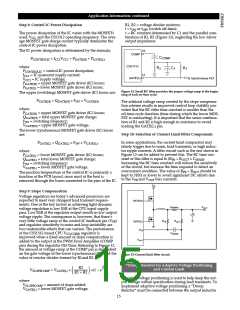
Step 5: Selection of the Input Capacitors
VCIN(RMS) = ICIN(RMS) × ESRCIN
,
These components must be selected and placed carefully to
yield optimal results. Capacitors should be chosen to pro-
vide acceptable ripple on the input supply lines. A key
specification for input capacitors is their ripple current rat-
ing. The input capacitor should also be able to handle the
where
VCIN(RMS) = input capacitor RMS voltage;
ICIN(RMS) = total input RMS current;
ESRCIN = total input capacitor ESR.
input RMS current IIN(RMS)
.
The designer must determine the input capacitor power
loss in order to ensure there isn’t excessive power dissipa-
tion through these components. The following formula is
used:
The combination of the input capacitors CIN discharges
during the on-time.
The input capacitor discharge current is given by:
PCIN(RMS) = ICIN(RMS)2 × ESRCIN
12

 CHERRY [ CHERRY SEMICONDUCTOR CORPORATION ]