Application Information: continued
When driving large capacitive loads, the COMP must
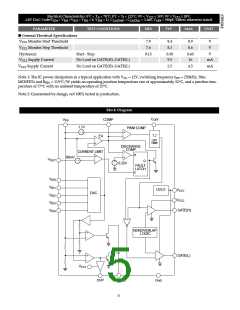
Protection and Monitoring Features
charge slowly enough to avoid tripping the CS51312 over-
current protection. The following equation can be used to
ensure unconditional startup:
Over-Current Protection
A hiccup mode current limit protection feature is provided,
requiring only the COMP capacitor to implement. The
CS51312 provides overcurrent protection by sensing the
current through a “Droop” resistor, using an internal cur-
rent sense comparator. The comparator compares the volt-
age drop through the “Droop” resistor to an internal refer-
ence voltage of 86mV (typical).
If the voltage drop across the “Droop” resistor exceeds this
threshold, the current sense comparator allows the fault
latch to be set. This causes the regulator to stop switching.
During this over current condition, the CS51312 stays off
for the time it takes the COMP pin capacitor to discharge
to its lower 0.25V threshold. As soon as the COMP pin
reaches 0.25V, the Fault latch is reset (no overcurrent con-
dition present) and the COMP pin is charged with a 30µA
current source to a voltage 1.1V greater than the VFB volt-
age. Only at this point the regulator attempts to restart nor-
mally by delivering short gate pulses to both FETS. This
protection scheme minimizes thermal stress to the regula-
tor components, input power supply, and PC board traces,
as the over current condition persists. Upon removal of the
overload, the fault latch is cleared, allowing normal opera-
tion to resume.
ICHG
I
LIM − ILOAD
<
CCOMP
COUT
where
CHG = COMP Source Current (30µA typical);
CCOMP = COMP Capacitor value (0.1µF typical);
ILIM = Current Limit Threshold;
ILOAD = Load Current during startup;
OUT = Total Output Capacitance.
I
C
Normal Operation
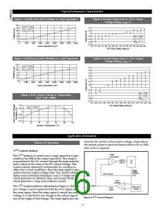
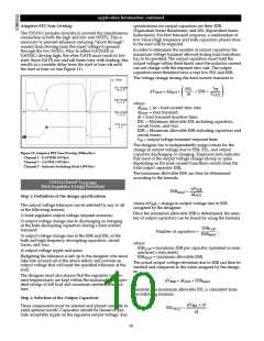
During Normal operation, Switch Off-Time is constant and
set by the COFF capacitor. Switch On-Time is adjusted by
the V2TM Control loop to maintain regulation. This results
in changes in regulator switching frequency, duty cycle,
and output ripple in response to changes in load and line.
Output voltage ripple will be determined by inductor rip-
ple current and the ESR of the output capacitors
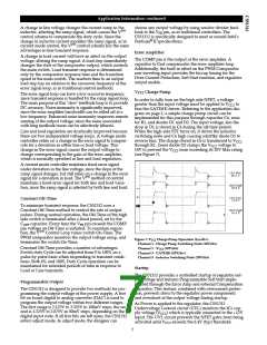
Transient Response
The CS51312 V2TM Control Loop’s 200ns reaction time pro-
vides unprecedented transient response to changes in
input voltage or output current. Pulse-by-pulse adjustment
of duty cycle is provided to quickly ramp the inductor cur-
rent to the required level. Since the inductor current cannot
be changed instantaneously, regulation is maintained by
the output capacitor(s) during the time required to slew the
inductor current.
Overall load transient response is further improved
through a feature called “Adaptive Voltage Positioning”.
This technique pre-positions the output capacitors voltage
to reduce total output voltage excursions during changes
in load.
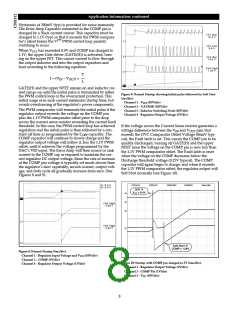
Holding tolerance to 1% allows the error amplifiers refer-
ence voltage to be targeted +25mV high without compro-
mising DC accuracy. A “Droop Resistor” connects the
Error Amps feedback pin (VFB) to the output capacitors
and load and carries the output current. With no load,
there is no DC drop across this resistor, producing an out-
put voltage tracking the Error amps, including the +25mV
offset. When the full load current is delivered, a 50mV
drop is developed across this resistor. This results in out-
put voltage being offset -25mV low.
The benefit of Adaptive Voltage Positioning is that addi-
tional margin is provided for a load transient before reach-
ing the output voltage specification limits. When load cur-
rent suddenly increases from its minimum level, the out-
put capacitor is pre-positioned +25mV. Conversely, when
load current suddenly decreases from its maximum level,
the output capacitor is pre-positioned -25mV. For best
Transient Response, a combination of a number of high fre-
quency and bulk output capacitors are usually used.
Overvoltage Protection
Overvoltage protection (OVP) is provided as result of the
normal operation of the V2TM control topology and requires
no additional external components. The control loop
responds to an overvoltage condition within 200ns, causing
the top MOSFET to shut off, disconnecting the regulator
from its input voltage. This results in a “crowbar” action to
clamp the output voltage and prevents damage to the load.
The regulator will remain in this state until the overvoltage
condition ceases or the input voltage is pulled low.
Additionally, a dedicated Overvoltage protection (OVP)
output pin (pin 13) is provided in the CS51312. The OVP
signal will go high (overvoltage condition), if the output
voltage (VCC(CORE)) exceeds the regulation voltage by 8.5%
of the voltage set by the particular DAC code. The OVP pin
can source up to 25mA of current that can be used to drive
an SCR to crowbar the power supply.
Power-Good Circuit
The Power-Good pin (pin 14) is an open-collector signal
consistent with TTL DC specifications. It is externally
pulled up, and is pulled low (below 0.3V) when the regula-
tor output voltage typically exceeds ± 8.5% of the nominal
output voltage. Maximum output voltage deviation before
Power-Good is pulled low is ± 12%.
Output Enable
On/off control of the regulator outputs can be implement-
ed by pulling the COMP pins low. It is required to pull the
COMP pins below the 1.1V PWM comparator offset volt-
age in order to disable switching on the GATE drivers.
9

 CHERRY [ CHERRY SEMICONDUCTOR CORPORATION ]