CM6802
NO BLEED RESISTOR GREEN MODE PFC/PWM CONTROLLER COMBO
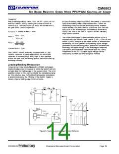
Error Amplifier Compensation
voltage amplifier, to prevent interaction with the voltage loop.
It should also be limited to less than 1/6th that of the
switching frequency, e.g. 16.7kHz for a 100kHz switching
frequency.
The PWM loading of the PFC can be modeled as a
negative resistor; an increase in input voltage to the PWM
causes a decrease in the input current. This response
dictates the proper compensation of the two
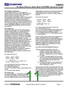
transconductance error amplifiers. Figure 2 shows the types
of compensation networks most commonly used for the
voltage and current error amplifiers, along with their
respective return points. The current loop compensation is
returned to VREF to produce a soft-start characteristic on the
PFC: as the reference voltage comes up from zero volts, it
creates a differentiated voltage on IEAO which prevents the
PFC from immediately demanding a full duty cycle on its
boost converter.
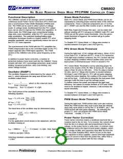
The Current Loop Gain (S)
∆VISENSE ∆DOFF
∆IEAO
=
≈
*
*
∆DOFF
OUTDC *R
∆IEAO ∆ISENSE
S *GM
* ZCI
V
I
S*L*2.5V
ZCI: Compensation Net Work for the Current Loop
GMI: Transconductance of IEAO
PFC Voltage Loop
V
OUTDC: PFC Boost Output Voltage; typical designed value is
There are two major concerns when compensating the
voltage loop error amplifier, VEAO; stability and transient
response. Optimizing interaction between transient
response and stability requires that the error amplifier’s
open-loop crossover frequency should be 1/2 that of the
line frequency, or 23Hz for a 47Hz line (lowest anticipated
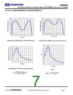
international power frequency). The gain vs. input voltage
of the CM6802’s voltage error amplifier, VEAO has a
specially shaped non-linearity such that under steady-state
operating conditions the transconductance of the error
amplifier is at a local minimum. Rapid perturbation in line or
load conditions will cause the input to the voltage error
amplifier (VFB) to deviate from its 2.5V (nominal) value. If
this happens, the transconductance of the voltage error
amplifier will increase significantly, as shown in the Typical
Performance Characteristics. This raises the
380V and we use the worst condition to calculate the ZCI
RS: The Sensing Resistor of the Boost Converter
2.5V: The Amplitude of the PFC Leading Modulation Ramp
L: The Boost Inductor
There is a modest degree of gain contouring applied to the
transfer characteristic of the current error amplifier, to
increase its speed of response to current-loop perturbations.
However, the boost inductor will usually be the dominant
factor in overall current loop response. Therefore, this
contouring is significantly less marked than that of the
voltage error amplifier. This is illustrated in the Typical
Performance Characteristics.
ISENSE Filter, the RC filter between RS and ISENSE
:
gain-bandwidth product of the voltage loop, resulting in a
much more rapid voltage loop response to such
perturbations than would occur with a conventional linear
gain characteristics.
There are 3 purposes to add a filter at ISENSE pin:
1.) Protection: During start up or inrush current
conditions, it will have a large voltage cross Rs
which is the sensing resistor of the PFC boost
converter. It requires the ISENSE Filter to attenuate
the energy.
The Voltage Loop Gain (S)
2.) To reduce L, the Boost Inductor: The ISENSE Filter
also can reduce the Boost Inductor value since the
ISENSE Filter behaves like an integrator before going
ISENSE which is the input of the current error
amplifier, IEAO.
∆VOUT
∆VFB ∆VEAO
=
≈
*
*
∆VEAO ∆VOUT
∆VFB
P
IN *2.5V
*GM *ZCV
V
V
OUTDC2 *∆VEAO *S*CDC
3.) By selecting the proper Rs, it can change the PFC
Green Mode threshold. Typical value is from 50
ohm (No Skipping) to 100 ohm.
Z
CV: Compensation Net Work for the Voltage Loop
GMv: Transconductance of VEAO
PIN: Average PFC Input Power
The ISENSE Filter is a RC filter. The resistor value of the ISENSE
Filter is between 100 ohm and 50 ohm because IOFFSET x the
resistor can generate an offset voltage of IEAO. By selecting
RFILTER equal to 50 ohm will keep the offset of the IEAO less
than 5mV. Usually, we design the pole of ISENSE Filter at
fpfc/6, one sixth of the PFC switching frequency. Therefore,
the boost inductor can be reduced 6 times without disturbing
the stability. Therefore, the capacitor of the ISENSE Filter,
CFILTER, will be around 283nF.
V
OUTDC: PFC Boost Output Voltage; typical designed value
is 380V.
CDC: PFC Boost Output Capacitor
PFC Current Loop
The current amplifier, IEAO compensation is similar to that of
the voltage error amplifier, VEAO with exception of the
choice of crossover frequency. The crossover frequency of
the current amplifier should be at least 10 times that of the
2003/06/25 Preliminary
Champion Microelectronic Corporation
Page 11

 CHAMP [ CHAMPION MICROELECTRONIC CORP. ]