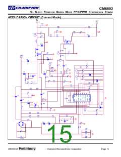
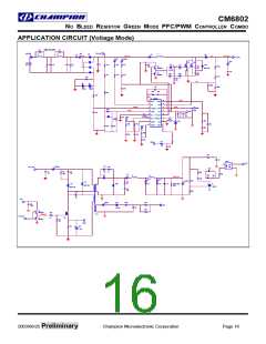
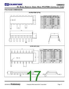
CM6802
NO BLEED RESISTOR GREEN MODE PFC/PWM CONTROLLER COMBO
EXAMPLE:
With a wanting voltage called, VBIAS ,of 18V, a VCC of 15V
and the CM6802 driving a total gate charge of 90nC at
100kHz (e.g. 1 IRF840 MOSFET and 2 IRF820 MOSFET),
the gate driver current required is:
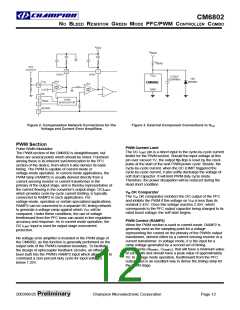
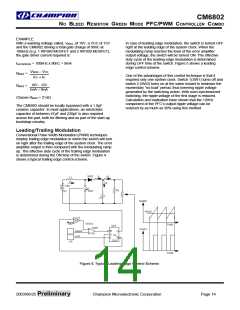
In case of leading edge modulation, the switch is turned OFF
right at the leading edge of the system clock. When the
modulating ramp reaches the level of the error amplifier
output voltage, the switch will be turned ON. The effective
duty-cycle of the leading edge modulation is determined
during OFF time of the switch. Figure 5 shows a leading
edge control scheme.
IGATEDRIVE = 100kHz x 90nC = 9mA
V
BIAS − VCC
I
RBIAS
=
=
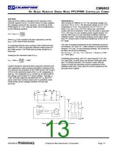
One of the advantages of this control technique is that it
required only one system clock. Switch 1(SW1) turns off and
switch 2 (SW2) turns on at the same instant to minimize the
momentary “no-load” period, thus lowering ripple voltage
generated by the switching action. With such synchronized
switching, the ripple voltage of the first stage is reduced.
Calculation and evaluation have shown that the 120Hz
component of the PFC’s output ripple voltage can be
reduced by as much as 30% using this method.
CC + I
G
18V −15V
5mA + 9mA
RBIAS
Choose RBIAS = 214Ω
The CM6802 should be locally bypassed with a 1.0µF
ceramic capacitor. In most applications, an electrolytic
capacitor of between 47µF and 220µF is also required
across the part, both for filtering and as part of the start-up
bootstrap circuitry.
Leading/Trailing Modulation
Conventional Pulse Width Modulation (PWM) techniques
employ trailing edge modulation in which the switch will turn
on right after the trailing edge of the system clock. The error
amplifier output is then compared with the modulating ramp
up. The effective duty cycle of the trailing edge modulation
is determined during the ON time of the switch. Figure 4
shows a typical trailing edge control scheme.
2003/06/25 Preliminary
Champion Microelectronic Corporation
Page 14

 CHAMP [ CHAMPION MICROELECTRONIC CORP. ]