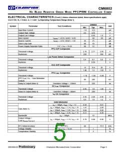
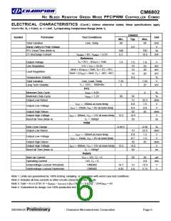
CM6802
NO BLEED RESISTOR GREEN MODE PFC/PWM CONTROLLER COMBO
Such supplies present a power factor to the line of less than
1. A current representing the instantaneous input voltage
(amplitude and waveshape) to the PFC. The rectified AC
input sine wave is converted to a proportional current via a
one (i.e. they cause significant current harmonics of the
power line frequency to appear at their input). If the input
current drawn by such a supply (or any other nonlinear
load) can be made to follow the input voltage in
resistor and is then fed into the gain modulator at IAC
.
Sampling current in this way minimizes ground noise, as is
required in high power switching power conversion
environments. The gain modulator responds linearly to this
current.
instantaneous amplitude, it will appear resistive to the AC
line and a unity power factor will be achieved.
To hold the input current draw of a device drawing power
from the AC line in phase with and proportional to the input
voltage, a way must be found to prevent that device from
loading the line except in proportion to the instantaneous
line voltage. The PFC section of the CM6802 uses a
boost-mode DC-DC converter to accomplish this. The input
to the converter is the full wave rectified AC line voltage. No
bulk filtering is applied following the bridge rectifier, so the
input voltage to the boost converter ranges (at twice line
frequency) from zero volts to the peak value of the AC input
and back to zero. By forcing the boost converter to meet
two simultaneous conditions, it is possible to ensure that
the current drawn from the power line is proportional to the
input line voltage. One of these conditions is that the output
voltage of the boost converter must be set higher than the
peak value of the line voltage. A commonly used value is
385VDC, to allow for a high line of 270VACrms. The other
condition is that the current drawn from the line at any given
instant must be proportional to the line voltage. Establishing
a suitable voltage control loop for the converter, which in
turn drives a current error amplifier and switching output
driver satisfies the first of these requirements. The second
requirement is met by using the rectified AC line voltage to
modulate the output of the voltage control loop. Such
modulation causes the current error amplifier to command a
power stage current that varies directly with the input
voltage. In order to prevent ripple, which will necessarily
appear at the output of boost circuit (typically about 10VAC
on a 385V DC level), from introducing distortion back
through the voltage error amplifier, the bandwidth of the
voltage loop is deliberately kept low. A final refinement is to
adjust the overall gain of the PFC such to be proportional to
1/VIN2, which linearizes the transfer function of the system
as the AC input to voltage varies.
2. A voltage proportional to the long-term RMS AC line
voltage, derived from the rectified line voltage after scaling
and filtering. This signal is presented to the gain modulator
at VRMS. The gain modulator’s output is inversely
proportional to VRMS2 (except at unusually low values of
VRMS where special gain contouring takes over, to limit
power dissipation of the circuit components under heavy
brownout conditions). The relationship between VRMS and
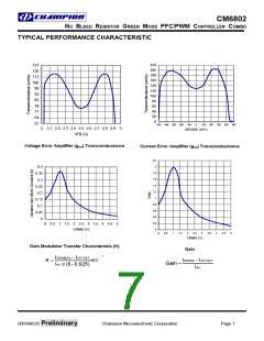
gain is called K, and is illustrated in the Typical
Performance Characteristics.
The output of the voltage error amplifier, VEAO. The gain
modulator responds linearly to variations in this voltage.
The output of the gain modulator is a current signal, in the
form of a full wave rectified sinusoid at twice the line
frequency. This current is applied to the virtual-ground
(negative) input of the current error amplifier. In this way the
gain modulator forms the reference for the current error loop,
and ultimately controls the instantaneous current draw of the
PFC form the power line. The general for of the output of the
gain modulator is:
I
AC× VEAO x 1V
IGAINMOD
=
(1)
2
V
RMS
More exactly, the output current of the gain modulator is
given by:
IGAINMOD = K x (VEAO – 0.625V) x IAC
Where K is in units of V-1
Note that the output current of the gain modulator is limited
around 228.47µA and the maximum output voltage of the
gain modulator is limited to 228.47uA x 3.5K=0.8V. This 0.8V
also will determine the maximum input power.
Since the boost converter topology in the CM6802 PFC is
of the current-averaging type, no slope compensation is
required.
However, IGAINMOD cannot be measured directly from ISENSE
ISENSE = IGAINMOD-IOFFSET and IOFFSET can only be measured
when VEAO is less than 0.5V and IGAINMOD is 0A. Typical
.
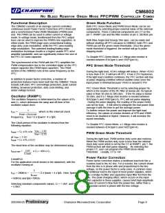
PFC Section
I
OFFSET is around 60uA.
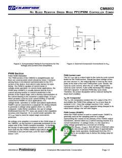
Gain Modulator
Figure 1 shows a block diagram of the PFC section of the
CM6802. The gain modulator is the heart of the PFC, as it
is this circuit block which controls the response of the
current loop to line voltage waveform and frequency, rms
line voltage, and PFC output voltages. There are three
inputs to the gain modulator. These are:
IAC
Typically, it has a feedforward resistor, RAC, less than 500K
ohm resistor connected between this pin and rectified line
input voltage.
During the startup condition, it supplies the startup current;
therefore, the system does not require additional bleed
resistor to start up the chip.
2003/06/25 Preliminary
Champion Microelectronic Corporation
Page 9

 CHAMP [ CHAMPION MICROELECTRONIC CORP. ]