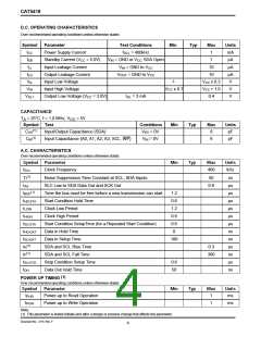
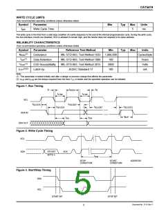
CAT5419
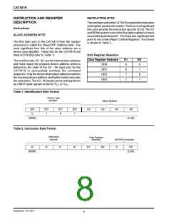
INSTRUCTION BYTE
INSTRUCTION AND REGISTER
DESCRIPTION
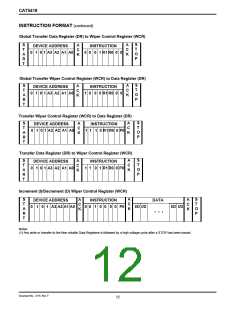
ThenextbytesenttotheCAT5419containstheinstruction
andregisterpointerinformation.Thefourmostsignificant
bits used provide the instruction opcode I [3:0]. The R1
and R0 bits point to one of the four data registers of each
associated potentiometer. The least two significant bits
point to one of two Wiper Control Registers. The format
is shown in Table 2.
Instructions
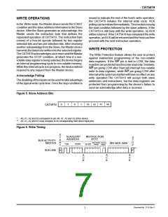
SLAVE ADDRESS BYTE
The first byte sent to the CAT5419 from the master/
processor is called the Slave/DPP Address Byte. The
most significant four bits of the slave address are a
device type identifier. These bits for the CAT5419 are
fixed at 0101[B] (refer to Table 1).
Data Register Selection
Data Register Selected
R1
0
R0
0
Thenextfourbits, A3-A0, aretheinternalslaveaddress
and must match the physical device address which is
defined by the state of the A3 - A0 input pins for the
CAT5419 to successfully continue the command
sequence.Onlythedevicewhichslaveaddressmatches
theincomingdeviceaddresssentbythemasterexecutes
the instruction. The A3 - A0 inputs can be actively driven
DR0
DR1
DR2
DR3
0
1
1
0
1
1
by CMOS input signals or tied to VCC or VSS
.
Table 1. Identification Byte Format
Device Type
Identifier
Slave Address
ID3
0
ID2
1
ID1
0
ID0
1
A3
A2
A1
A0
(MSB)
(LSB)
Table 2. Instruction Byte Format
Instruction
Opcode
Data Register
Selection
WCR/Pot Selection
I3
I2
I1
I0
R1
R0
0
P0
(MSB)
(LSB)
Document No. 2115, Rev. F
8

 CATALYST [ CATALYST SEMICONDUCTOR ]