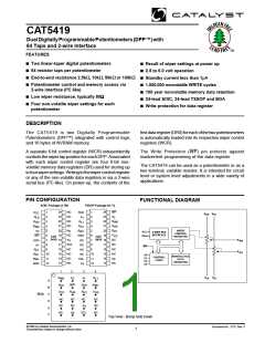
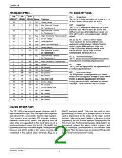
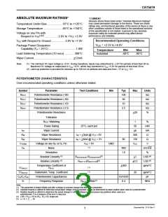
CAT5419
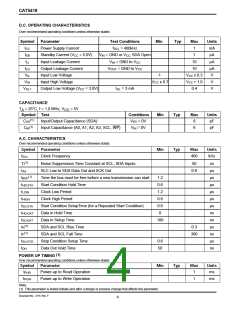
WRITE CYCLE LIMITS
Over recommended operating conditions unless otherwise stated.
Symbol
Parameter
Min
Typ
Max
Units
tWR
Write Cycle Time
5
ms
The write cycle is the time from a valid stop condition of a write sequence to the end of the internal program/erase cycle. During the write cycle,
the bus interface circuits are disabled, SDA is allowed to remain high, and the device does not respond to its slave address.
RELIABILITY CHARACTERISTICS
Over recommended operating conditions unless otherwise stated.
Symbol
Parameter
Reference Test Method
MIL-STD-883, Test Method 1033
MIL-STD-883, Test Method 1008
MIL-STD-883, Test Method 3015
JEDEC Standard 17
Min
1,000,000
100
Typ
Max
Units
Cycles/Byte
Years
(1)
NEND
Endurance
(1)
TDR
Data Retention
ESD Susceptibility
Latch-Up
(1)
VZAP
2000
Volts
(1)(2)
ILTH
100
mA
Note:
(1) This parameter is tested initially and after a design or process change that affects the parameter.
(2) t and t are the delays required from the time V is stable until the specified operation can be initiated.
PUR
PUW
CC
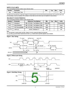
Figure 1. Bus Timing
t
t
t
R
F
HIGH
t
t
LOW
LOW
SCL
t
t
HD:DAT
SU:STA
t
t
t
t
HD:STA
SU:DAT
SU:STO
SDA IN
BUF
t
t
DH
AA
SDA OUT
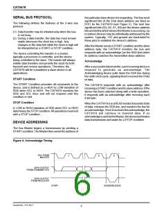
Figure 2. Write Cycle Timing
SCL
SDA
8TH BIT
BYTE n
ACK
t
WR
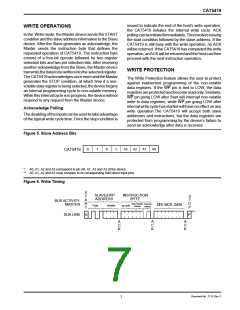
STOP
CONDITION
START
CONDITION
ADDRESS
Figure 3. Start/Stop Timing
SDA
SCL
START BIT
STOP BIT
Document No. 2115, Rev. F
5

 CATALYST [ CATALYST SEMICONDUCTOR ]