CAT5419
issued to indicate the end of the host's write operation,
the CAT5419 initiates the internal write cycle. ACK
pollingcanbeinitiatedimmediately.Thisinvolvesissuing
the start condition followed by the slave address. If the
CAT5419 is still busy with the write operation, no ACK
will be returned. If the CAT5419 has completed the write
operation, anACKwillbereturnedandthehostcanthen
proceed with the next instruction operation.
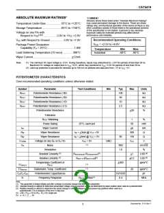
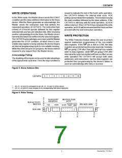
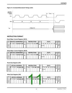
WRITE OPERATIONS
In the Write mode, the Master device sends the START
condition and the slave address information to the Slave
device. After the Slave generates an acknowledge, the
Master sends the instruction byte that defines the
requested operation of CAT5419. The instruction byte
consist of a four-bit opcode followed by two register
selection bits and two pot selection bits. After receiving
another acknowledge from the Slave, the Master device
transmitsthedatatobewrittenintotheselectedregister.
TheCAT5419acknowledgesoncemoreandtheMaster
generates the STOP condition, at which time if a non-
volatiledataregisterisbeingselected,thedevicebegins
an internal programming cycle to non-volatile memory.
Whilethisinternalcycleisinprogress, thedevicewillnot
respond to any request from the Master device.
WRITE PROTECTION
The Write Protection feature allows the user to protect
against inadvertent programming of the non-volatile
data registers. If the WP pin is tied to LOW, the data
registersareprotectedandbecomereadonly. Similarly,
WP pin going LOW after Start will interrupt non-volatile
write to data registers, while WP pin going LOW after
internal write cycle has started will have no effect on any
write operation.The CAT5419 will accept both slave
addresses and instructions, but the data registers are
protected from programming by the device’s failure to
send an acknowledge after data is received.
Acknowledge Polling
Thedisablingoftheinputscanbeusedtotakeadvantage
of the typical write cycle time. Once the stop condition is
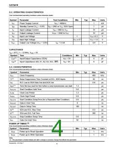
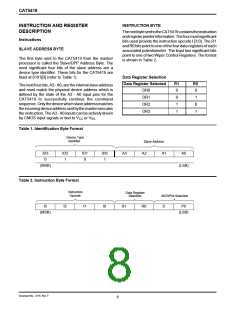
Figure 5. Slave Address Bits
0
1
0
1
A3
A2
A1
A0
CAT5419
*
A0, A1, A2 and A3 correspond to pin A0, A1, A2 and A3 of the device.
** A0, A1, A2 and A3 must compare to its corresponding hard wired input pins.
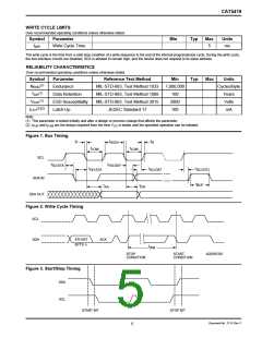
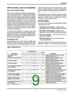
Figure 6. Write Timing
S
SLAVE/DPP
ADDRESS
INSTRUCTION
BYTE
T
A
R
T
S
T
O
P
BUS ACTIVITY:
MASTER
Data Register
Pot/WCR
Address
DR1 WCR DATA
Fixed
Variable
op code
Address
SDA LINE
S
P
A
C
K
A
C
K
A
C
K
Document No. 2115, Rev. F
7

 CATALYST [ CATALYST SEMICONDUCTOR ]