CAT5419
exchange data between the WCR and one of the Data
Registers. The WCR controls the position of the wiper.
The response of the wiper to this action will be delayed
bytWRL.AtransferfromtheWCR(currentwiperposition),
to a Data Register is a write to non-volatile memory and
takes a maximum of tWR to complete. The transfer can
occur between one of the potentiometers and one of its
associated registers; or the transfer can occur between
all potentiometers and one associated register.
— Global XFR Data Register to Wiper
Control Register
This transfers the contents of specified Data
Registers to the associated Wiper Control
Registers.
— Global XFR Wiper Counter Register to
Data Register
This transfers the contents of all Wiper Control
Registers to the specified associated Data
Registers.
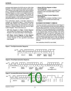
Four instructions require a two-byte sequence to
complete, as illustrated in Figure 7. These instructions
transfer data between the host/processor and the
CAT5419; either between the host and one of the data
registers or directly between the host and the Wiper
Control Register. These instructions are:
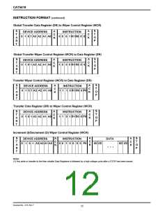
INCREMENT/DECREMENT COMMAND
The final command is Increment/Decrement (Figure 5
and 9). The Increment/Decrement command is different
from the other commands. Once the command is issued
and the CAT5419 has responded with an acknowledge,
the master can clock the selected wiper up and/or down
in one segment steps; thereby providing a fine tuning
— XFR Data Register to Wiper Control Register
This transfers the contents of one specified Data
Register to the associated Wiper Control Register.
capability to the host. For each SCL clock pulse (tHIGH
)
while SDA is HIGH, the selected wiper will move one
resistor segment towards the RH terminal. Similarly, for
each SCL clock pulse while SDA is LOW, the selected
wiper will move one resistor segment towards the RL
terminal.
— XFR Wiper Control Register to Data Register
This transfers the contents of the specified Wiper
Control Register to the specified associated
Data Register.
See Instructions format for more detail.
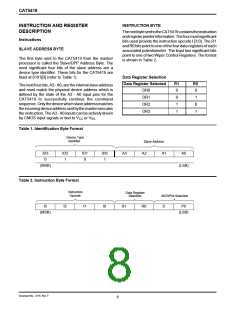
Figure 7. Two-Byte Instruction Sequence
SDA
0
1
0
1
ID3 ID2 ID1 ID0
S
A2 A1 A0
S
T
A
R
T
A3
A I3 I2 I1
I0
R1 R0
0
P0
A
C
K
C
K
T
O
P
Internal
Address
Instruction
Opcode
Register
Address
Pot/WCR
Address
Device ID
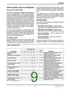
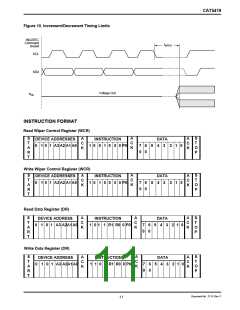
Figure 8. Three-Byte Instruction Sequence
SDA
0
1
0
1
S
T
A
R
T
I3
ID3 ID2
ID0
A
C
K
I2
I1
I0 R1 R0
0
P0
A
C
K
D7 D6 D5 D4 D3 D2 D1 D0
A
C
K
S
T
O
P
ID1
A3 A2 A1 A0
Internal
Address
Device ID
WCR[7:0]
or
Data Register D[7:0]
Instruction
Opcode
Data
Register Address
Pot/WCR
Address
Figure 9. Increment/Decrement Instruction Sequence
0
1
0
1
SDA
ID3 ID2 ID1 ID0
Device ID
I1
A3 A2 A1 A0
I3
I2
I0
R1 R0
0
P0
S
T
A
R
T
A
C
K
A
C
K
I
I
D
E
C
1
S
T
O
P
I
D
E
C
n
N
C
1
N
C
2
N
C
n
Internal
Address
Instruction
Opcode
Pot/WCR
Address
Data
Register
Address
Document No. 2115, Rev. F
10

 CATALYST [ CATALYST SEMICONDUCTOR ]