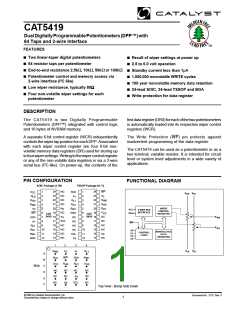
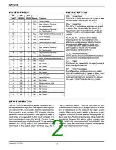
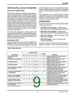
CAT5419
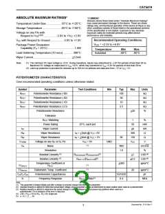
ABSOLUTE MAXIMUM RATINGS*
*COMMENT
Stresses above those listed under “Absolute Maximum Ratings”
may cause permanent damage to the device. These are stress
ratings only, and functional operation of the device at these or any
other conditions outside of those listed in the operational sections
of this specification is not implied. Exposure to any absolute
maximum rating for extended periods may affect device
performance and reliability.
Temperature Under Bias .................. -55°C to +125°C
Storage Temperature........................ -65°C to +150°C
Voltage on any Pin with
Respect to VSS(1)(2) ................ -2.0V to +VCC +2.0V
Recommended Operating Conditions:
VCC with Respect to Ground ................ -2.0V to +7.0V
V
CC
= +2.5V to +6.0V
Package Power Dissipation
Capability (TA = 25°C) ................................... 1.0W
Temperature
Min
Max
Lead Soldering Temperature (10 secs) ............ 300°C
Industrial
-40°C
85°C
Wiper Current.................................................. +12mA
Note:
(1) The minimum DC input voltage is –0.5V. During transitions, inputs may undershoot to –2.0V for periods of less than 20 ns.
Maximum DC voltage on output pins is V +0.5V, which may overshoot to V +2.0V for periods of less than 20 ns.
CC
CC
(2) Latch-up protection is provided for stresses up to 100 mA on address and data pins from –1V to V +1V.
CC
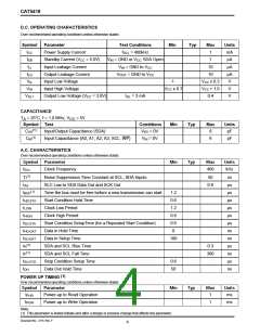
POTENTIOMETER CHARACTERISTICS
Over recommended operating conditions unless otherwise stated.
Symbol
RPOT
Parameter
Test Conditions
Min
Typ
100
50
Max
Units
kΩ
Potentiometer Resistance (-00)
Potentiometer Resistance (-50)
Potentiometer Resistance (-10)
Potentiometer Resistance (-2.5)
Potentiometer Resistance
RPOT
kΩ
RPOT
10
kΩ
RPOT
2.5
kΩ
+20
%
Tolerance
RPOT Matching
1
%
mW
mA
Power Rating
25°C, each pot
50
IW
RW
Wiper Current
+6
Wiper Resistance
Wiper Resistance
Voltage on any RH or RL Pin
Noise
IW = +3mA @ VCC =3V
IW = +3mA @ VCC = 5V
300
150
VCC
Ω
RW
80
Ω
VTERM
VN
VSS = 0V
GND
V
(1)
TBD
1.6
nV/ Hz
%
Resolution
Absolute Linearity (2)
Relative Linearity (3)
Rw(n)(actual)-R(n)(expected)
+1
LSB (4)
LSB (4)
ppm/°C
(5)
(5)
Rw(n+1)-[Rw(n)+LSB
]
+0.2
Temperature Coefficient of
RPOT
+300
(1)
(1)
(1)
TCRPOT
TCRATIO
CH/CL/CW
fc
Ratiometric Temp. Coefficient
Potentiometer Capacitances
Frequency Response
20
ppm/°C
pF
10/10/25
0.4
RPOT = 50kΩ(1)
MHz
Note:
(1) This parameter is tested initially and after a design or process change that affects the parameter.
(2) Absolute linearity is utilitzed to determine actual wiper voltage versus expected voltage as determined by wiper position when used as a potentiometer.
(3) Relative linearity is utilized to determine the actual change in voltage between two successive tap positions when used as a
potentiometer. It is a measure of the error in step size.
(4) LSB = RTOT / 63 or (RH - RL) / 63, single pot
(5) n = 0, 1, 2, ..., 63
Document No. 2115, Rev. F
3

 CATALYST [ CATALYST SEMICONDUCTOR ]