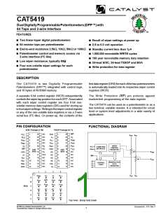
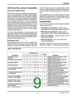
CAT5419
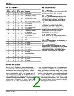
PIN DESCRIPTION
PIN DESCRIPTIONS
Pin
Pin
Pin
SCL:
Serial Clock
(TSSOP) (SOIC) (BGA) Name Function
The CAT5419 serial clock input pin is used to clock
all data transfers into or out of the device.
19
20
1
2
C1
B1
VCC
RL0
Supply Voltage
Low Reference Terminal
for Potentiometer 0
SDA:
Serial Data
The CAT5419 bidirectional serial data pin is used
to transfer data into and out of the device. The
SDA pin is an open drain output and can be wire-
OR'd with the other open drain or open collector
outputs.
21
3
C2
RH0
High Reference Terminal
for Potentiometer 0
22
23
24
1
4
5
6
7
8
9
A1
A2
B2
B3
A3
A4
RW0
A2
Wiper Terminal for Potentiometer 0
Device Address
A0, A1, A2, A3: Device Address Inputs
These inputs set the device address when
addressing multiple devices. A total of sixteen
devices can be addressed on a single bus.
A match in the slave address must be made
with the address input in order to initiate
communication with the CAT5419.
WP
SDA
A1
Write Protection
Serial Data Input/Output
Device Address
2
3
RL1
Low Reference Terminal
for Potentiometer 1
4
10
C3
RH1
High Reference Terminal
for Potentiometer 1
RH, RL: Resistor End Points
The RH and RL pins are equivalent to the terminal
connections on a mechanical potentiometer.
5
11
12
13
14
15
16
17
18
19
20
21
22
23
B4
C4
D4
E4
D3
F4
F3
E3
D1
F2
F1
D2
E1
RW1
GND
NC
NC
NC
NC
SCL
A3
Wiper Terminal for Potentiometer 1
Ground
6
RW:
Wiper
The RW pins are equivalent to the wiper terminal of
a mechanical potentiometer.
7
No Connect
8
No Connect
WP:
Write Protect Input
9
No Connect
The WP pin when tied low prevents non-volatile
writes to the data registers (change of wiper control
register is allowed) and when tied high or left
floating normal read/write operations are allowed.
See page 7, Write Protection for more details.
10
11
12
13
14
15
16
17
No Connect
Bus Serial Clock
Device Address
No Connect
NC
A0
Device Address, LSB
No Connect
NC
NC
NC
No Connect
No Connect
18
24
E2
NC
No Connect
DEVICE OPERATION
The CAT5419 is two resistor arrays integrated with 2-
wireserialinterfacelogic,four6-bitwipercontrolregisters
and sixteen 6-bit, non-volatile memory data registers.
Each resistor array contains 63 separate resistive
elements connected in series. The physical ends of
each array are equivalent to the fixed terminals of a
mechanical potentiometer (RH and RL). RH and RL are
symmetricalandmaybeinterchanged.Thetappositions
between and at the ends of the series resistors are
connected to the output wiper terminals (RW) by a
CMOS transistor switch. Only one tap point for each
potentiometerisconnectedtoitswiperterminalatatime
and is determined by the value of the wiper control
register. Data can be read or written to the wiper control
registers or the non-volatile memory data registers via
the 2-wire bus. Additional instructions allow data to be
transferred between the wiper control registers and
each respective potentiometer's non-volatile data
registers. Also, the device can be instructed to operate
in an "increment/decrement" mode.
Document No. 2115, Rev. F
2

 CATALYST [ CATALYST SEMICONDUCTOR ]