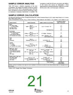
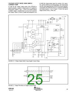
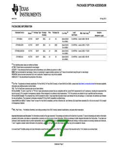
VOLTAGE OUTPUT MODE USING SIMPLE
CURRENT PUMP
to build this charge pump using two resistors, two capaci-
tors, and two diodes (in an SOT package). The charge pump
uses the clock signal from the XTR108 SCLK pin to operate;
consequently, the XTR108 must be in continuous EEPROM
read mode (register 4, bit 0). Figure 15 shows the typical
output of this circuit (–50mV dc).
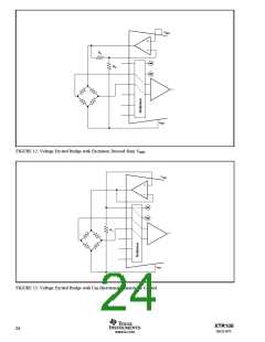
In order for the voltage output mode of the XTR108 to
operate properly, a negative voltage needs to be applied to
the IRET pin (–200mV < IRET < –25mV). For systems without
a negative supply a charge pump is an easy way to generate
this voltage. Figure 14 shows a simple and inexpensive way
VOUT = −50mV
BAV99
36.5kΩ
1nF
OPA –IN
OPA +IN
CS1 CS2 SDIO SCLK
30kΩ 330pF
XTR108
SPI and
Control Circuits
OPA OUT
REFIN
OSC
Voltage
Reference
REFOUT
IREF
Σ
DAC
+5V
ILIN
VGate
DAC
Sub-Regulator
VS
Driver
1
2
−200mV < VOA+ < −25mV
Zero
DAC
Q1
V/I-0
V/I-1
V/I-2
Output
Current
Amplifier
IQ1 = 0mA
DSUB
PGA
V/I-3
V/I-4
V/I-5
0mV
RZ1 RZ2 RZ3 RZ4 RZ5
2.5kΩ
51Ω
Linearization
Circuit
IO
RTD
CFILT
0.01µF
RLIN
RSET
VOUT
IIN
IRET
RCM
15.8kΩ
12.1kΩ
VOUT
FIGURE 14. Voltage Output Mode Using Simple Current Pump.
XTR108
SCLK
5.0V
−50mV
Charge
Pump
Output
FIGURE 15. Output Waveform of Simple Current Pump.
XTR108
SBOS187C
25
www.ti.com

 BB [ BURR-BROWN CORPORATION ]