TSC2005
www.ti.com
SBAS379–DECEMBER 2006
DIGITAL INTERFACE
The TSC2005 communicates through a standard SPI bus. The SPI allows full-duplex, synchronous, serial
communication between a host processor (the master) and peripheral devices (slaves). The SPI master
generates the synchronizing clock and initiates transmissions. The SPI slave devices depend on a master to
start and synchronize transmissions.
A transmission begins when initiated by a master SPI. The byte from the master SPI begins shifting in on the
slave SDI (MOSI—master out, slave in) pin under the control of the master serial clock. As the byte shifts in on
the SDI (MOSI) pin, a byte shifts out on the SDO (MISO—master in, slave out) pin to the master shift register.
The idle state of the TSC2005 serial clock is logic low, which corresponds to a clock polarity setting of 0 (typical
microprocessor SPI control bit CPOL = 0). The TSC2005 interface is designed so that with a clock phase bit
setting of 0 (typical microprocessor SPI control bit CPHA = 0), the master begins driving its MOSI pin and the
slave begins driving its MISO pin half an SCLK before the first serial clock edge. The CS (SS, slave select) pin
can remain low between transmissions.
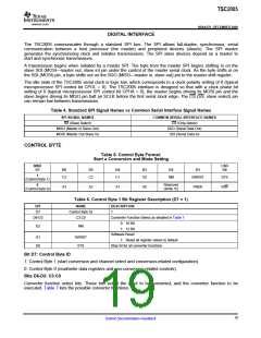
Table 4. Standard SPI Signal Names vs Common Serial Interface Signal Names
SPI SIGNAL NAMES
SS (Slave Select)
COMMON SERIAL INTERFACE NAMES
CS (Chip Select)
MISO (Master In Slave Out)
MOSI (Master Out Slave In)
SDO (Serial Data Out)
SDI (Serial Data In)
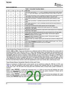
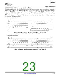
CONTROL BYTE
Table 5. Control Byte Format:
Start a Conversion and Mode Setting
MSB
D7
LSB
D0
D6
D5
D4
D3
D2
D1
1
C3
C2
C1
C0
RM
SWRST
STS
R/W
(Control Byte 1)
0
Reserved
(Write '0')
A3
A2
A1
A0
PND0
(Control Byte 0)
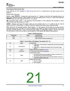
Table 6. Control Byte 1 Bit Register Description (D7 = 1)
BIT
D7
NAME
Control Byte ID
C3:C0
DESCRIPTION
1
D6-D3
Converter Function Select as detailed in Table 7
0: 10 Bit
D2
RM
1: 12 Bit
Software Reset
D1
D0
SWRST
STS
1: Reset all register values to default
Stop bit for all converter functions
Bit D7: Control Byte ID
1: Control Byte 1 (start conversion and channel select and conversion-related configuration).
0: Control Byte 0 (read/write data registers and non-conversion-related controls).
Bits D6-D3: C3:C0
Converter function select bits. These bits select the input to be converted, and the converter function to be
executed. Table 7 lists the possible converter functions.
19
Submit Documentation Feedback

 BB [ BURR-BROWN CORPORATION ]