PDF
最近搜索
热门搜索
发布采购

| 型号: | PCM1804 |
| PDF下载: | 下载PDF文件 查看货源 |
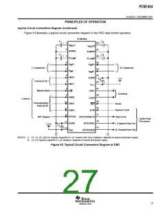
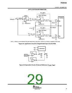
| 内容描述: | 全差分模拟输入24位, 192千赫立体声A / D转换器 [FULL DIFFERENTIAL ANALOG INPUT 24-BIT, 192-kHz STEREO A/D CONVERTER] |
| 分类和应用: | 转换器输入元件 |
| 文件页数/大小: | 31 页 / 470 K |
| 品牌: |  BB [ BURR-BROWN CORPORATION ] BB [ BURR-BROWN CORPORATION ] |
专业IC领域供求交易平台:提供全面的IC Datasheet资料和资讯,Datasheet 1000万数据,IC品牌1000多家。