PCM1804
SLES022A – DECEMBER 2001
PRINCIPLES OF OPERATION
theory of operation
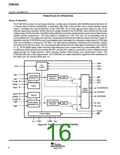
The PCM1804 consists of a band-gap reference, a delta-sigma modulator with full differential architecture for
L-channel and R-channel respectively, a decimation filter with a low-cut filter, and a serial interface circuit.
Figure 1 illustrates the total architecture of the PCM1804. An on-chip high-precision reference with 10-µF
external capacitor(s) provides all the reference voltage needed in the PCM1804, and it defines the full-scale
voltagerangeofbothchannels. Fulldifferentialarchitectureprovidesawidedynamicrangeandexcellentpower
supply rejection performance. The input signal is sampled at ×128, ×64, and ×32 oversampling rate for
oversampling ratio. The single rate, dual rate, and quad rate eliminate the external sample-hold amp. Figure 31
illustrates how the PCM1804 for each oversampling ratio decimates the modulator output down to PCM data
when the modulator is running at 6.144 MHz. The delta-sigma modulation randomizes the modulator outputs
and reduces the idle tone level. The oversampled data stream from the delta-sigma modulator is converted to
a 1 f , 24-bit digital signal, while removing high-frequency noise components by a decimation filter. The dc
S
components of the signal are removed by the HPF, and the HPF output is converted to a time-multiplexed serial
signal through the serial interface, which provides flexible serial formats and master/slave modes. The
PCM1804 also has a DSD output mode. The PCM1804 can output directly the signal from the modulators to
the DSDL (pin 16) and the DSDR (pin 15).
OSR0
CLK
Control
SCKI
OSR1
OSR2
V
IN
L+
Delta-Sigma
Decimation
Filter (L)
HPF
S/M
Modulator (L)
V
L–
IN
FMT0
FMT1
V
L
COM
AGNDL
V
REF
L
V
REF
L
LRCK/DSDBCK
BCK/DSDL
Serial
Output
Interface
V
R
REF
AGNDR
V R
REF
DATA/DSDR
V
COM
R
V
R+
Decimation
Filter (R)
IN
Delta-Sigma
Modulator (R)
OVFL
OVFR
HPF
V
R–
IN
BYPAS
RST
Power Supply
V
CC
AGND
DGND
V
DD
Figure 30. Total Block Diagram of PCM1804
16
www.ti.com

 BB [ BURR-BROWN CORPORATION ]