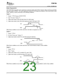
ꢀ
ꢁ
ꢂ
ꢃ
ꢄ
ꢅ
ꢆ
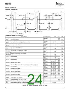
www.ti.com
SLES100 − DECEMBER 2003
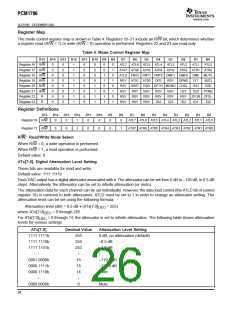
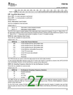
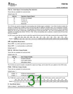
B15 B14 B13 B12 B11 B10
Register 18 R/W
B9
B8
B7
B6
B5
B4
B3
B2
B1
B0
0
0
1
0
0
1
0
ATLD FMT2 FMT1 FMT0 DMF1 DMF0 DME MUTE
R/W: Read/Write Mode Select
When R/W = 0, a write operation is performed.
When R/W = 1, a read operation is performed.
Default value: 0
ATLD: Attenuation Load Control
This bit is available for read and write.
Default value: 0
ATLD = 0
ATLD = 1
Attenuation control disabled (default)
Attenuation control enabled
The ATLD bit is used to enable loading of the attenuation data contained in registers 16 and 17. When ATLD = 0,
the attenuation settings remain at the previously programmed levels, ignoring new data loaded from registers 16 and
17. When ATLD = 1, attenuation data written to registers 16 and 17 is loaded normally.
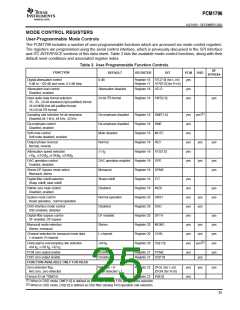
FMT[2:0]: Audio Interface Data Format
These bits are available for read and write.
Default value: 101
FMT[2:0]
000
Audio Data Format Selection
16-bit standard format, right-justified data
20-bit standard format, right-justified data
24-bit standard format, right-justified data
24-bit MSB-first, left-justified format data
001
010
011
2
100
16-bit I S format data
2
101
24-bit I S format data (default)
110
Reserved
Reserved
111
The FMT[2:0] bits are used to select the data format for the serial audio interface.
For the external digital filter interface mode (DFTH mode), this register is operated as shown in the APPLICATION
FOR EXTERNAL DIGITAL FILTER INTERFACE section of this data sheet.
DMF[1:0]: Sampling Frequency Selection for the De-Emphasis Function
These bits are available for read and write.
Default value: 00
DMF[1:0]
De-Emphasis Sampling Frequency Selection
00
01
10
11
Disabled (default)
48 kHz
44.1 kHz
32 kHz
The DMF[1:0] bits are used to select the sampling frequency used by the digital de-emphasis function when it is
enabled by setting the DME bit. The de-emphasis curves are shown in the TYPICAL PERFORMANCE CURVES
section of this data sheet.
For the DSD mode, analog FIR filter performance can be selected using this register. A register map and filter
response plots are shown in the APPLICATION FOR DSD FORMAT (DSD MODE) INTERFACE section of this data
sheet.
27

 BB [ BURR-BROWN CORPORATION ]