ꢀ
ꢁ
ꢂ
ꢃ
ꢄ
ꢅ
ꢆ
www.ti.com
SLES100 − DECEMBER 2003
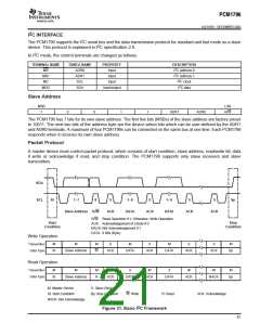
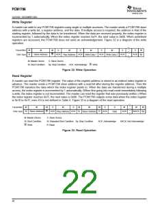
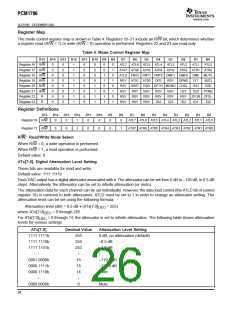
Write Register
A master can write to any PCM1796 registers using single or multiple accesses. The master sends a PCM1796 slave
address with a write bit, a register address, and the data. If multiple access is required, the address is that of the
starting register, followed by the data to be transferred. When the data are received properly, the index register is
incremented by 1 automatically. When the index register reaches 0x7F, the next value is 0x00. When undefined
registers are accessed, the PCM1796 does not send an acknowledgement. Figure 32 is a diagram of the write
operation.
Transmitter
M
M
M
M
S
M
S
M
S
M
S
S
Data Type St
Sp
Slave Address
W
ACK
ACK
ACK
ACK
ACK
Reg Address
Write Data 1
Write Data 2
M: Master Device
S: Slave Device
St: Start Condition
Sp: Stop Condition ACK: Acknowledge W: Write
Figure 32. Write Operation
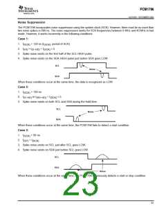
Read Register
A master can read the PCM1796 register. The value of the register address is stored in an indirect index register in
advance. The master sends a PCM1796 slave address with a read bit after storing the register address. Then the
PCM1796 transfers the data which the index register points to. When the data are transferred during a multiple
access, the index register is incremented by 1 automatically. (When first going into read mode immediately following
a write, the index register is not incremented. The master can read the register that was previously written.) When
the index register reaches 0x7F, the next value is 0x00. The PCM1796 outputs some data when the index register
is 0x10 to 0x1F, even if it is not defined in Table 4. Figure 33 is a diagram of the read operation.
Transmitter
M
M
M
M
S
M
S
M
M
M
S
S
M
M
Data Type St
Sp
Slave Address
W
ACK
ACK Sr
R
ACK
ACK
NACK
Reg Address
Slave Address
Data
M: Master Device
St: Start Condition
W: Write
S: Slave Device
Sr: Repeated Start Condition Sp: Stop Condition
R: Read
ACK: Acknowledge
NACK: Not Acknowledge
Figure 33. Read Operation
22

 BB [ BURR-BROWN CORPORATION ]