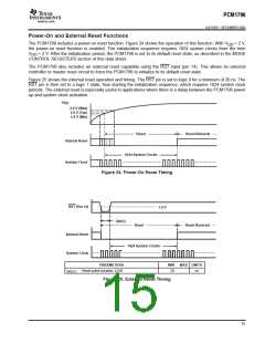
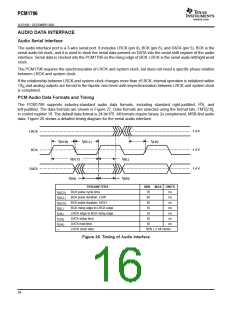
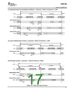
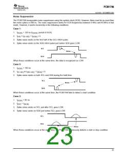
ꢀ
ꢁ
ꢂ
ꢃ
ꢄ
ꢅ
ꢆ
www.ti.com
SLES100 − DECEMBER 2003
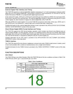
SERIAL CONTROL INTERFACE
2
The PCM1796 supports SPI and I C that sets mode control registers as shown in Table 4. This serial control interface
2
is selected by MSEL (pin 3), SPI is activated when MSEL is set to LOW, and I C is activated when MSEL is set to
HIGH.
SPI Interface
The SPI interface is a 4-wire synchronous serial port that operates asynchronously to the serial audio interface and
the system clock (SCK). The serial control interface is used to program and read the on-chip mode registers. The
control interface includes MDO (pin 13), MDI (pin 11), MC (pin 12), and MS (pin 10). MDO is the serial data output,
used to read back the values of the mode registers; MDI is the serial data input, used to program the mode registers;
MC is the serial bit clock, used to shift data in and out of the control port, and MS is the mode control enable, used
to enable the internal mode register access.
Register Read/Write Operation
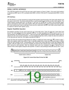
All read/write operations for the serial control port use 16-bit data words. Figure 28 shows the control data word
format. The most significant bit is the read/write (R/W) bit. For write operations, the R/W bit must be set to 0. For
read operations, the R/W bit must be set to 1. There are seven bits, labeled IDX[6:0], that hold the register index (or
address) for the read and write operations. The least significant eight bits, D[7:0], contain the data to be written to,
or the data that was read from, the register specified by IDX[6:0].
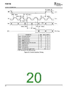
Figure 29 shows the functional timing diagram for writing or reading the serial control port. MS is held at a logic 1
state until a register needs to be written or read. To start the register write or read cycle, MS is set to logic 0. Sixteen
clocks are then provided on MC, corresponding to the 16 bits of the control data word on MDI and readback data
on MDO. After the eighth clock cycle has completed, the data from the indexed-mode control register appears on
MDO during the read operation. After the sixteenth clock cycle has completed, the data is latched into the
indexed-mode control register during the write operation. To write or read subsequent data, MS must be set to 1 once.
LSB
D0
MSB
R/W IDX6 IDX5 IDX4 IDX3 IDX2 IDX1 IDX0
D7
D6
D5
D4
D3
D2
D1
Register Index (or Address)
Register Data
Figure 28. Control Data Word Format for MDI
MS
MC
MDI
MDO
R/W A6 A5 A4 A3
A2 A1 A0 D7 D6 D5 D4
D3 D2 D1 D0
High Impedance
D7 D6 D5 D4
D3 D2 D1 D0
When Read Mode is Instructed
NOTE: Bit 15 is used for selection of write or read. Setting R/W = 0 indicates a write, while R/W = 1 indicates a read. Bits 14−8 are used for the register
address. Bits 7–0 are used for register data.
Figure 29. Serial Control Format
19

 BB [ BURR-BROWN CORPORATION ]