SERIAL PERIPHERAL INTERFACE
CS is used to select the device. It can be used to decode the
ADS1218 in systems where a number of parts are connected
to the serial bus.
The Serial Peripheral Interface (SPI), allows a controller to
communicate synchronously with the ADS1218. The
ADS1218 operates in slave only mode.
The timing specification shows the timing diagram for
interfacing to the ADS1218 with CS used to decode the part.
SPI Transfer Formats
The ADS1218 serial interface can operate in three-wire
mode by tying the CS input LOW. In this case, the SCLK,
DIN, and DOUT lines are used to communicate with the
ADS1218 and the status of DRDY can be obtained by
interrogating bit 7 of the M/DEC1 register. This scheme is
suitable for interfacing to microcontrollers. If CS is required
as a decoding signal, it can be generated from a port pin.
During an SPI transfer, data is simultaneously transmitted
and received. The SCLK signal synchronizes shifting and
sampling of the information on the two serial data lines: DIN
and DOUT. The CS signal allows individual selection of an
ADS1218 device; an ADS1218 with CS HIGH is not active
on the bus.
Clock Phase and Polarity Controls (POL)
The clock polarity is specified by the POL pin, which selects
an active HIGH or active LOW clock, and has no effect on
the transfer format.
DEFINITION OF TERMS
Analog Input Voltage—the voltage at any one analog input
relative to AGND.
Serial Clock (SCLK)
Analog Input Differential Voltage—given by the following
equation: (IN+ – IN–). Thus, a positive digital output is pro-
duced whenever the analog input differential voltage is posi-
tive, while a negative digital output is produced whenever the
differential is negative.
SCLK, a Schmitt Trigger input to the ADS1218, is gener-
ated by the master device and synchronizes data transfer on
the DIN and DOUT lines. When transferring data to or from
the ADS1218, burst mode may be used i.e., multiple bits of
data may be transferred back-to-back with no delay in
SCLKs or toggling of CS.
For example, when the converter is configured with a 2.5V
reference and placed in a gain setting of 1, the positive
full-scale output is produced when the analog input differen-
tial is 2.5V. The negative full-scale output is produced when
the differential is –2.5V. In each case, the actual input
voltages must remain within the AGND to AVDD range.
Chip Select (CS)
The chip select (CS) input of the ADS1218 must be exter-
nally asserted before a master device can exchange data with
the ADS1218. CS must be LOW before data transactions
and must stay LOW for the duration of the transaction.
Conversion Cycle—the term “conversion cycle” usually
refers to a discrete A/D conversion operation, such as that
performed by a successive approximation converter. As
used here, a conversion cycle refers to the tDATA time period.
However, each digital output is actually based on the modu-
lator results from several tDATA time periods.
DIGITAL INTERFACE
The ADS1218’s programmable functions are controlled
using a set of on-chip registers, as outlined previously. Data
is written to these registers via the part’s serial interface and
read access to the on-chip registers is also provided by this
interface.
FILTER SETTING
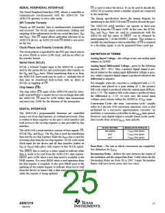
fast settling
sinc2
MODULATOR RESULTS
1 tDATA time period
2 tDATA time period
3 tDATA time period
The ADS1218’s serial interface consists of four signals: CS,
SCLK, DIN, and DOUT. The DIN line is used for transferring
data into the on-chip registers while the DOUT line is used for
accessing data from the on-chip registers. SCLK is the serial
clock input for the device and all data transfers (either on
DIN or DOUT) take place with respect to this SCLK signal.
sinc3
Data Rate—The rate at which conversions are completed.
See definition for fDATA
.
The DRDY line is used as a status signal to indicate when
data is ready to be read from the ADS1218’s data register.
DRDY goes LOW when a new data word is available in the
DOR register. It is reset HIGH when a read operation from
the data register is complete. It also goes HIGH prior to the
updating of the output register to indicate when not to read
from the device to ensure that a data read is not attempted
while the register is being updated.
Decimation Ratio—defines the ratio between the output of
the modulator and the output Data Rate. Valid values for the
Decimation Ratio are from 20 to 2047. Larger Decimation
Ratios will have lower noise and vice-versa.
ADS1218
25
SBAS187

 BB [ BURR-BROWN CORPORATION ]