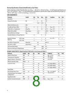
Package Characteristics
Parameter
Symbol
Device
Min.
Typ.
Max.
Units
Conditions
Note
Input-Output Momentary
Withstand Voltage*
VISO
HCPL-7860 3750
HCPL-786J 5000
1012
Vrms
RH ≤ 50%, t = 1 min; 19, 20
TA = 25°C
Input-Output Resistance
RI-O
1013
ꢆ
V
I-O = 500 Vdc
20
1011
TA = 100°C
f = 1 MHz
Input-Output Capacitance
CI-O
1.4
96
pF
20
Input IC Junction-to-Case
Thermal Resistance
ꢇjci
°C/W
Thermocouple located at center
underside of package
Output IC Junction-to-Case
Thermal Resistance
ꢇjco
114
°C/W
*The Input-Output Momentary Withstand Voltage is a dielectric voltage rating that should not be interpreted as an input-output continuous voltage
rating. For the continuous voltage rating refer to the IEC/EN/DIN EN 60747-5-2 Insulation Characteristics Table (if applicable), your equipment level
safety specification, or Avago Technologies Application Note 1074, “Optocoupler Input-Output Endurance Voltage.”
Notes:
1. If V (pin 3) is brought above V
- 2 V with respect to GND1 an internal optical-coupling test mode may be activated. This test mode is not
IN-
DD1
intended for customer use.
2. All units within each HCPL-7860 standard packaging increment (either 50 per tube or 1000 per reel) have a Reference Voltage Matching of 1%.
An Absolute Reference Voltage Tolerance of 4% is guaranteed between standard packaging increments.
3. Because of the switched-capacitor nature of the isolated modulator, time averaged values are shown.
4. CMRR is defined as the ratio of the gain for differential inputs applied between V and V to the gain for common-mode inputs applied to both
IN
IN+
IN-
V
IN+
and V with respect to input ground GND1.
IN-
5. Short-circuit current is the amount of output current generated when either output is shorted to V
recommended.
or GND2. Use under these conditions is not
DD2
6. Data hold time is amount of time that the data output MDAT will stay stable following the rising edge of output clock MCLK.
7. Resolution is defined as the total number of output bits. The useable accuracy of any A/D converter is a function of its linearity and signal-to-noise
ratio, rather than how many total bits it has.
8. Integral nonlinearity is defined as one-half the peak-to-peak deviation of the best-fit line through the transfer curve for V = -200 mV to +200 mV,
IN+
expressed either as the number of LSBs or as a percent of measured input range (400 mV).
9. Differential nonlinearity is defined as the deviation of the actual difference from the ideal difference between midpoints of successive output codes,
expressed in LSBs.
10. Data sheet value is the average magnitude of the difference in offset voltage from T =25°C to T = 85°C, expressed in microvolts per °C. Three
A
A
standard deviation from typical value is less than 6 ꢄV/°C.
11. Beyond the full-scale input range the output is either all zeroes or all ones.
12. The effective number of bits (or effective resolution) is defined by the equation ENOB = (SNR-1.76)/6.02 and represents the resolution of an ideal,
quantization-noise limited A/D converter with the same SNR.
13. Conversion time is defined as the time from when the convert start signal CS is brought low to when SDAT goes high, indicating that output data
is ready to be clocked out. This can be as small as a few cycles of the isolated modulator clock and is determined by the frequency of the isolated
modulator clock and the selected Conversion and Pre-Trigger modes. For determining the true signal delay characteristics of the A/D converter for
closed-loop phase margin calculations, the signal delay specification should be used.
14. Signal delay is defined as the effective delay of the input signal through the Isolated A/D converter. It can be measured by applying a -200 mV to
200 mV step at the input of modulator and adjusting the relative delay of the convert start signal CS so that the output of the converter is at mid
scale. The signal delay is the elapsed time from when the step signal is applied at the input to when output data is ready at the end of the conver-
sion cycle. The signal delay is the most important specification for determining the true signal delay characteristics of the A/D converter and should
be used for determining phase margins in closed-loop applications. The signal delay is determined by the frequency of the modulator clock and
which Conversion Mode is selected, and is independent of the selected Pre-Trigger Mode and, therefore, conversion time.
15. The minimum and maximum overrange detection time is determined by the frequency of the channel 1 isolated modulator clock.
16. The minimum and maximum threshold detection time is determined by the user-defined configuration of the adjustable threshold detection circuit
and the frequency of the channel 1 isolated modulator clock. See the Applications Information section for further detail. The specified times apply
for the default configuration.
17. The signal bandwidth is the frequency at which the magnitude of the output signal has decreased 3 dB below its low-frequency value. The signal
bandwidth is determined by the frequency of the modulator clock and the selected Conversion Mode.
18. The isolation transient immunity (also known as Common-Mode Rejection) specifies the minimum rate-of-rise of an isolation-mode signal applied
across the isolation boundary beyond which the modulator clock or data signals are corrupted.
19. In accordance with UL1577, for devices with minimum V specified at 3750 Vrms(HCPL-7860) or 5000 Vmrs (HCPL-786J) , each isolated modulator
ISO
(optocoupler) is proof-tested by applying an insulation test voltage greater than 4500 Vrms (HCPL-7860) or 6000 Vrms (HCPl-786J) for one second.
This test is performed before the Method b, 100% production test for partial discharge shown in IEC/EN/DIN EN 60747-5-2 Insulation Characteristics
Table.
20. This is a two-terminal measurement: pins 1-4 are shorted together and pins 5-8 are shorted together.
9

 AVAGO [ AVAGO TECHNOLOGIES LIMITED ]