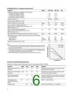
Absolute Maximum Ratings
Parameter
Symbol
Min.
Max.
Units
Note
Storage Temperature
TS
-55
125
°C
Ambient Operating Temperature
Supply Voltages
TA
-40
0
85
°C
V
VDD1, VDD2
5.5
Steady-State Input Voltage
Two Second Transient Input Voltage
Output Voltages
VIN+, VIN-
-2.0
-6.0
-0.5
VDD1 + 0.5
V
1
MCLK, MDAT
V
DD2 + 0.5
V
Lead Solder Temperature
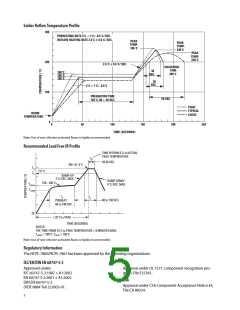
Solder Reflow Temperature Profile
260°C for 10 sec., 1.6 mm below seating plane
See Maximum Solder Reflow Thermal Profile section
Recommended Operating Conditions
Parameter
Symbol
Min.
Max.
Units
Note
Ambient Operating Temperature
TA
-40
+85
°C
Supply Voltages
Input Voltage
VDD1, VDD2
4.5
5.5
V
VIN+, VIN-
-200
+200
mV
1
Electrical Specifications (DCꢀ
Unless otherwise noted, all specifications are at V = 0 V and V = 0 V, all Typical specifications are at T = 25°C and
IN+
IN-
A
V
DD1
V
DD1
= V
= 5 V, and all Minimum and Maximum specifications apply over the following ranges: T = -40°C to +85°C,
D
D
2
A
= 4.5 to 5.5 V and V
= 4.5 to 5.5 V.
DD2
Parameter
Symbol
Min.
Typ.
Max.
Units
Conditions
Fig.
Note
Average Input Bias Current
IIN
-0.8
ꢀA
1
3
Average Input Resistance
RIN
450
60
k ꢆ
3
4
Input DC Common-Mode
Rejection Ratio
CMRRIN
dB
Output Logic High Voltage
Output Logic Low Voltage
Output Short Circuit Current
VOH
VOL
3.9
4.9
0.1
30
V
IOUT = -100 ꢀA
IOUT = 1.6 mA
0.6
V
|IOSC
|
mA
VOUT = VDD2
or GND2
5
6
Input Supply Current
Output Supply Current
Output Clock Frequency
Data Hold Time
IDD1
IDD2
fCLK
10
10
10
15
15
mA
mA
MHz
ns
VIN+ = -350 mV
to +350 mV
2
3
4
15
8.2
13.2
tHDDAT
7

 AVAGO [ AVAGO TECHNOLOGIES LIMITED ]