3
Electrical Specifications (Tested with HCPL-0872 or Sinc Filterꢀ
Unless otherwise noted, all specifications are at V = -200 mV to +200 mV and V = 0 V; all Typical specifications are
IN+
IN-
at T = 25°C and V
= V
= 5 V, and all Minimum and Maximum specifications apply over the following ranges: T =
A
DD1
D
D
2
A
-40°C to +85°C, V
= 4.5 to 5.5 V and V
= 4.5 to 5.5 V.
DD1
DD2
STATIC CHARACTERISTICS
Parameter
Symbol
Min.
Typ.
Max.
Units
Conditions
Fig. Note
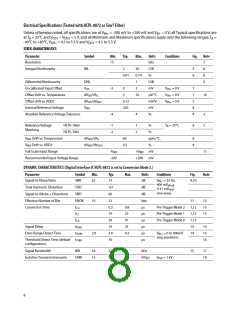
Resolution
15
bits
7
Integral Nonlinearity
INL
3
30
0.14
1
LSB
%
5
6
8
8
9
0.01
Differential Nonlinearity
DNL
VOS
LSB
mV
ꢀV/°C
mV/V
mV
%
Uncalibrated Input Offset
Offset Drift vs. Temperature
Offset drift vs. VDD1
-3
0
3
VIN+ = 0 V
VIN+ = 0 V
VIN+ = 0 V
7
7
7
8
8
dVOS/dTA
dVOS/dVDD1
VREF
2
10
10
0.12
320
Internal Reference Voltage
Absolute Reference Voltage Tolerance
-4
4
2
2
Reference Voltage
Matching
HCPL-7860
HCPL-786J
-1
-2
1
2
%
TA = 25°C.
8
%
V
REF Drift vs. Temperature
dVREF/dTA
60
ppm/°C.
%
8
8
VREF Drift vs. VDD1
dVREF/dVDD1
0.2
Full Scale Input Range
-VREF
-200
+VREF mV
+200 mV
11
Recommended Input Voltage Range
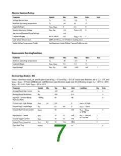
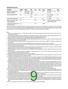
DYNAMIC CHARACTERISTICS (Digital Interface IC HCPL-0872 is set to Conversion Mode 3.ꢀ
Parameter
Symbol
Min.
Typ.
Max.
Units
Conditions
Fig.
Note
Signal-to-Noise Ratio
SNR
62
73
dB
VIN+ = 35 Hz,
400 mVpk-pk
9,10
Total Harmonic Distortion
Signal-to-(Noise + Distortion)
Effective Number of Bits
Conversion Time
THD
SND
ENOB
tC2
-67
66
12
0.2
19
39
19
3.0
10
dB
dB
bits
ꢀs
(141 mVrms
)
sine wave.
10
11
12
13
13
0.8
23
47
23
4.2
Pre-Trigger Mode 2
Pre-Trigger Mode 1
Pre-Trigger Mode 0
1,12
1,12
1,12
13
tC1
ꢀs
tC0
ꢀs
Signal Delay
tDSIG
tOVR1
ꢀs
14
15
16
Over-Range Detect Time
2.0
ꢀs
VIN+ = 0 to 400mV
step waveform
14
Threshold Detect Time (default tTHR1
configuration)
ꢀs
Signal Bandwidth
BW
18
15
22
20
kHz
15
17
18
Isolation Transient Immunity
CMR
kV/ꢀs
VISO = 1 kV
8

 AVAGO [ AVAGO TECHNOLOGIES LIMITED ]