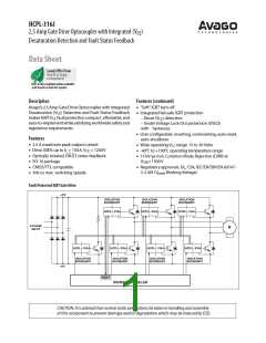
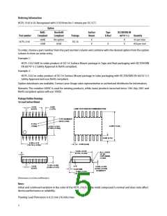
Package Pin Out
1
2
3
4
5
6
7
8
V
V
V
V
16
15
IN+
IN-
E
V
LED2+
DESAT 14
CC1
GND1
V
13
12
11
10
9
CC2
RESET
FAULT
V
C
V
OUT
V
V
V
V
LED1+
LED1-
EE
EE
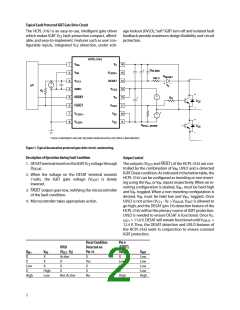
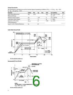
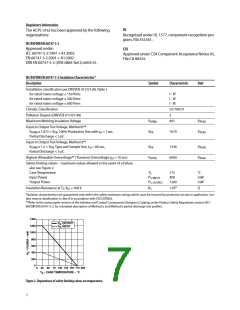
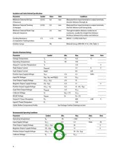
Pin Descriptions
Symbol Description
Symbol
Description
VIN+
Noninverting gate drive voltage output (VOUT
control input.
)
VE
Common (IGBT emitter) output supply voltage.
VIN-
Inverting gate drive voltage output
(VOUT) control input.
VLED2+
DESAT
LED 2 anode. This pin must be left unconnected
for guaranteed data sheet performance. (For
optical coupling testing only.)
VCC1
Positive input supply voltage. (4.5 V to 5.5 V)
Desaturation voltage input. When the voltage
on DESAT exceeds an internal reference
voltage of 7V while the IGBT is on, FAULT
output is changed from a high impedance
state to a logic low state within 5 µs. See
Note 25.
GND1
RESET
Input Ground.
VCC2
VC
Positive output supply voltage.
FAULT reset input. A logic low input for at least
0.1 µs, asynchronously resets FAULT output high
and enables VIN. Synchronous control of RESET
relative to VIN is required. RESET is not affected
by UVLO. Asserting RESET while VOUT is high does
Collector of output pull-up triple-darlington
transistor. It is connected to VCC2 directly or
through a resistor to limit output turn-on
current.
not affect VOUT
.
FAULT
Fault output. FAULT changes from a high
impedance state to a logic low output within
5 µs of the voltage on the DESAT pin exceeding
an internal reference voltage of 7V. FAULT
output remains low until RESET is brought low.
FAULT output is an open collector which allows
the FAULT outputs from all HCPL-316Js in a
circuit to be connected together in a “wired OR”
forming a single fault bus for interfacing directly
to the micro-controller.
VOUT
Gate drive voltage output.
VLED1+
LED 1 anode. This pin must be left unconnected
for guaranteed data sheet performance. (For
optical coupling testing only.)
VEE
Output supply voltage.
VLED1-
LED 1 cathode. This pin must be connected to
ground.
4

 AVAGO [ AVAGO TECHNOLOGIES LIMITED ]