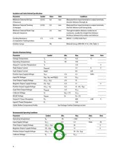
Insulation and Safety Related Specifications
Parameter
Symbol
Value
Units
Conditions
Minimum External Air Gap
(Clearance)
L(101)
8.3
mm
Measured from input terminals to output terminals,
shortest distance through air.
Minimum External Tracking
(Creepage)
L(102)
8.3
0.5
mm
mm
Measured from input terminals to output terminals,
shortest distance path along body.
Minimum Internal Plastic Gap
(Internal Clearance)
Through insulation distance conductor to
conductor, usually the straight line distance
thickness between the emitter and detector.
Tracking Resistance
(Comparative Tracking Index)
CTI
>175
IIIa
Volts
DIN IEC 112/VDE 0303 Part 1
Isolation Group
Material Group (DIN VDE 0110, 1/89, Table 1)
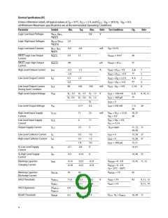
Absolute Maximum Ratings
Parameter
Symbol
Min.
-55
-40
Max.
125
Units
Note
Storage Temperature
Ts
°C
Operating Temperature
Output IC Junction Temperature
Peak Output Current
TA
100
TJ
125
4
5
|Io(peak)
IFAULT
VCC1
|
2.5
A
Fault Output Current
8.0
mA
Volts
Positive Input Supply Voltage
Input Pin Voltages
-0.5
5.5
VIN+, VIN- and VRESET
(VCC2 - VEE
(VE - VEE
-0.5
VCC1
35
Total Output Supply Voltage
Negative Output Supply Voltage
Positive Output Supply Voltage
Gate Drive Output Voltage
Collector Voltage
)
-0.5
)
-0.5
15
6
4
(VCC2 - VE)
Vo(peak)
VC
-0.5
35 - (VE - VEE
VCC2
VCC2
VE + 10
600
)
-0.5
VEE + 5 V
VE
DESAT Voltage
VDESAT
PO
Output IC Power Dissipation
Input IC Power Dissipation
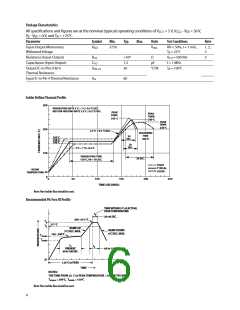
Solder Reflow Temperature Profile
mW
PI
150
See Package Outline Drawings section
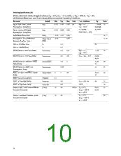
Recommended Operating Conditions
Parameter
Symbol
TA
Min.
-40
4.5
Max.
Units
Note
Operating Temperature
Input Supply Voltage
+100
°C
VCC1
5.5
Volts
28
9
Total Output Supply Voltage
Negative Output Supply Voltage
Positive Output Supply Voltage
Collector Voltage
(VCC2 - VEE
)
15
30
(VE - VEE
)
0
15
6
(VCC2 - VE)
VC
15
30 - (VE - VEE
)
VEE + 6
VCC2
8

 AVAGO [ AVAGO TECHNOLOGIES LIMITED ]