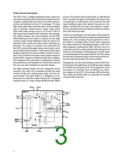
Product Overview Description
The HCPL-316J is a highly integrated power control de-
vice that incorporates all the necessary components for a
complete, isolated IGBT gate drive circuit with fault pro-
tection and feedback into one SO-16 package. TTL input
logic levels allow direct interface with a microcontroller,
and an optically isolated power output stage drives
IGBTs with power ratings of up to 150 A and 1200 V. A
high speed internal optical link minimizes the propaga-
tion delays between the microcontroller and the IGBT
while allowing the two systems to operate at very large
common mode voltage differences that are common in
industrial motor drives and other power switching ap-
plications. An output IC provides local protection for
the IGBT to prevent damage during overcurrents, and a
second optical link provides a fully isolated fault status
feedback signal for the microcontroller. A built in“watch-
dog” circuit monitors the power stage supply voltage to
prevent IGBT caused by insufficient gate drive voltages.
This integrated IGBT gate driver is designed to increase
the performance and reliability of a motor drive without
the cost, size, and complexity of a discrete design.
process. The forward optical signal path, as indicated by
LED1, transmits the gate control signal. The return opti-
cal signal path, as indicated by LED2, transmits the fault
status feedback signal. Both optical channels are com-
pletely controlled by the input and output ICs respec-
tive-ly, making the internal isolation boundary transpar-
ent to the microcontroller.
Under normal operation, the input gate control signal di-
rectly controls the IGBT gate through the isolated output
detector IC. LED2 remains off and a fault latch in the in-
put buffer IC is disabled. When an IGBT fault is detected,
the output detector IC immediately begins a “soft” shut-
down sequence, reducing the IGBT current to zero in a
controlled manner to avoid potential IGBT damage from
inductive overvoltages. Simultaneously, this fault status
is transmitted back to the input buffer IC via LED2, where
the fault latch disables the gate control input and the ac-
tive low fault output alerts the microcontroller.
During power-up, the UnderVoltage Lockout (UVLO) fea-
ture prevents the application of insufficient gate voltage
to the IGBT, by forcing the HCPL-316J’s output low. Once
Two light emitting diodes and two integrated circuits
housed in the same SO-16 package provide the input
control circuitry, the output power stage, and two op-
tical channels. The input Buffer IC is designed on a bi-
polar process, while the output Detector IC is designed
manufactured on a high voltage BiCMOS/Power DMOS
the output is in the high state, the DESAT (V ) detec-
CE
tion feature of the HCPL-316J provides IGBT protection.
Thus, UVLO and DESAT work in conjunction to provide
constant IGBT protection.
V
V
LED1-
LED1+
7
8
13
INPUT IC
V
V
CC2
C
12
1
2
V
V
IN+
LED1
D
R
I
V
E
R
IN-
UVLO
11
14
V
OUT
DESAT
3
V
CC1
DESAT
9,10
16
V
V
EE
E
SHIELD
LED2
5
6
RESET
FAULT
FAULT
SHIELD
OUTPUT IC
4
15
V
GND1
LED2+
3

 AVAGO [ AVAGO TECHNOLOGIES LIMITED ]