IPM Dead Time and Propagation Delay Specifications.
(Discussion applies to HCPL-3120, HCPL-J312, and
HCNW3120)
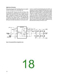
Under Voltage Lockout Feature. (Discussion applies to
HCPL-3120, HCPL-J312, and HCNW3120)
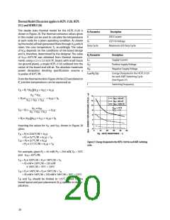
TheꢀHCPL-3120ꢀcontainsꢀanꢀunderꢀvoltageꢀlockoutꢀ(UVLO)ꢀ
featureꢀthatꢀisꢀdesignedꢀtoꢀprotectꢀtheꢀIGBTꢀunderꢀfaultꢀ
conditionsꢀwhichꢀ causeꢀtheꢀ HCPL-3120ꢀsupplyꢀvoltageꢀ
(equivalentꢀ toꢀ theꢀ fully-chargedꢀ IGBTꢀ gateꢀ voltage)ꢀ toꢀ
dropꢀbelowꢀaꢀlevelꢀnecessaryꢀtoꢀkeepꢀtheꢀIGBTꢀinꢀaꢀlowꢀre-
sistanceꢀstate.ꢀWhenꢀtheꢀHCPL-3120ꢀoutputꢀisꢀinꢀtheꢀhighꢀ
stateꢀandꢀtheꢀsupplyꢀvoltageꢀdropsꢀbelowꢀtheꢀꢀꢀꢀꢀHCPL-
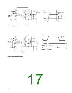
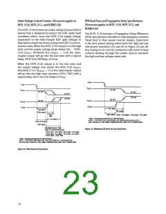
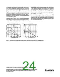
TheꢀHCPL-3120ꢀincludesꢀaꢀPropagationꢀDelayꢀDifferenceꢀ
(PDD)ꢀspecificationꢀintendedꢀtoꢀhelpꢀdesignersꢀminimizeꢀ
“deadꢀtime”ꢀinꢀtheirꢀpowerꢀinverterꢀdesigns.ꢀDeadꢀtimeꢀ
isꢀtheꢀtimeꢀperiodꢀduringꢀwhichꢀbothꢀtheꢀhighꢀandꢀlowꢀ
sideꢀpowerꢀtransistorsꢀ(Q1ꢀandꢀQ2ꢀinꢀFigureꢀ25)ꢀareꢀoff.ꢀ
AnyꢀoverlapꢀinꢀQ1ꢀandꢀQ2ꢀconductionꢀwillꢀresultꢀinꢀlargeꢀ
currentsꢀ flowingꢀ throughꢀ theꢀ powerꢀ devicesꢀ betweenꢀ
theꢀhighꢀandꢀlowꢀvoltageꢀmotorꢀrails.
3120ꢀ V ꢀ thresholdꢀ (9.5ꢀ<
UVLO–
V
<ꢀ 12.0)ꢀ theꢀ opto-
UVLO–ꢀ
couplerꢀoutputꢀwillꢀgoꢀintoꢀtheꢀlowꢀstateꢀwithꢀaꢀtypicalꢀ
delay,ꢀUVLOꢀTurnꢀOffꢀDelay,ꢀofꢀ0.6ꢀµs.
Whenꢀ theꢀ HCPL-3120ꢀ outputꢀ isꢀ inꢀ theꢀ lowꢀ stateꢀ andꢀ
theꢀ supplyꢀ voltageꢀ risesꢀ aboveꢀ theꢀ HCPL-3120ꢀ V
ꢀ
UVLO+
thresholdꢀ(11.0ꢀ<
V
ꢀ<ꢀ13.5)ꢀtheꢀoptocouplerꢀoutputꢀ
UVLO+
willꢀgoꢀintoꢀtheꢀhighꢀstateꢀ(assumesꢀLEDꢀisꢀ“ON”)ꢀwithꢀaꢀ
typicalꢀdelay,ꢀUVLOꢀTurnꢀOnꢀDelayꢀofꢀ0.8ꢀµs.
I
LED1
I
LED1
V
OUT1
V
Q1 ON
OUT1
Q1 ON
Q1 OFF
Q3 ON
Q1 OFF
Q3 ON
Q3 OFF
V
Q3 OFF
OUT3
V
OUT3
I
LED3
I
LED3
t
PHL MAX
t
PHL MIN
t
PLH MIN
t
PHL MAX
t
PLH
MIN
PDD* MAX = (t - t
ꢁ
= t
- t
PHL MAX PLH MIN
PHL PLH MAX
*PDD = PROPAGATION DELAY DIFFERENCE
NOTE: FOR PDD CALCULATIONS THE PROPAGATION DELAYS
ARE TAKEN AT THE SAME TEMPERATURE AND TEST CONDITIONS.
t
PLH MAX
(t
t
ꢁ
PHL- PLH MAX
PDD* MAX
MAXIMUM DEAD TIME
Figure 35. Minimum LED skew for zero dead time.
(DUE TO OPTOCOUPLERꢁ
= (t
= (t
- t
ꢁ + (t
- t
ꢁ
PHL MAX PHL MIN
PLH MAX PLH MIN
- t ꢁ – (t
- t ꢁ
PHL MAX PLH MIN
PHL MIN PLH MAX
= PDD* MAX – PDD* MIN
*PDD = PROPAGATION DELAY DIFFERENCE
NOTE: FOR DEAD TIME AND PDD CALCULATIONS ALL PROPAGATION
DELAYS ARE TAKEN AT THE SAME TEMPERATURE AND TEST CONDITIONS.
Figure 36. Waveforms for dead time.
23

 AVAGO [ AVAGO TECHNOLOGIES LIMITED ]