Thermal Model (Discussion applies to HCPL-3120, HCPL-
J312 and HCNW3120)
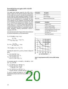
Theꢀ steadyꢀ stateꢀ thermalꢀ modelꢀ forꢀ theꢀ HCPL-3120ꢀ isꢀ
shownꢀinꢀFigureꢀ28.ꢀTheꢀthermalꢀresistanceꢀvaluesꢀgivenꢀ
inꢀthisꢀmodelꢀcanꢀbeꢀusedꢀtoꢀcalculateꢀtheꢀtemperaturesꢀ
atꢀeachꢀnodeꢀforꢀaꢀgivenꢀoperatingꢀcondition.ꢀAsꢀshownꢀ
P Parameter
Description
E
IFꢀ
LEDꢀCurrent
VFꢀ
LEDꢀOnꢀVoltage
MaximumꢀLEDꢀDutyꢀCycle
byꢀtheꢀmodel,ꢀallꢀheatꢀgeneratedꢀflowsꢀthroughꢀq whichꢀ
CAꢀ
DutyꢀCycleꢀ
raisesꢀ theꢀ caseꢀ temperatureꢀ T ꢀ accordingly.ꢀ Theꢀ valueꢀ
C
ofꢀq ꢀdependsꢀonꢀtheꢀconditionsꢀofꢀtheꢀboardꢀdesignꢀ
CA
andꢀis,ꢀtherefore,ꢀdeterminedꢀbyꢀtheꢀdesigner.ꢀTheꢀvalueꢀ
P Parameter
Description
O
ofꢀ q ꢀ=ꢀ83°C/Wꢀ wasꢀ obtainedꢀ fromꢀ thermalꢀ measure-
CA
ICC
ꢀ
SupplyꢀCurrent
mentsꢀusingꢀaꢀ2.5ꢀxꢀ2.5ꢀinchꢀPCꢀboard,ꢀwithꢀsmallꢀtracesꢀ
(noꢀgroundꢀplane),ꢀaꢀsingleꢀHCPL-3120ꢀsolderedꢀintoꢀtheꢀ
centerꢀofꢀtheꢀboardꢀandꢀstillꢀair.ꢀTheꢀabsoluteꢀmaximumꢀ
powerꢀ dissipationꢀ deratingꢀ specificationsꢀ assumeꢀ aꢀ
VCC
ꢀ
PositiveꢀSupplyꢀVoltage
NegativeꢀSupplyꢀVoltage
EnergyꢀDissipatedꢀinꢀtheꢀHCPL-3120ꢀ
forꢀeachꢀIGBTꢀSwitchingꢀCycleꢀꢀ
(SeeꢀFigureꢀ27)
VEEꢀ
ESW(Rg,Qg)ꢀ
ꢀ
ꢀ
q valueꢀofꢀ83°C/W.
CA
ꢀ
FromꢀtheꢀthermalꢀmodeꢀinꢀFigureꢀ28ꢀtheꢀLEDꢀandꢀdetectorꢀ
ICꢀjunctionꢀtemperaturesꢀcanꢀbeꢀexpressedꢀas:
fꢀ
SwitchingꢀFrequency
@ꢀ
T ꢀ=ꢀP (q ||(q ꢀ+ꢀq )ꢀ+ꢀq
)
CA
JE
Eꢀ
LC LD
DC
ꢀ ꢀ ꢀ ꢀ ꢀꢀq ꢀ*ꢀq
LC
DC
14
13
10
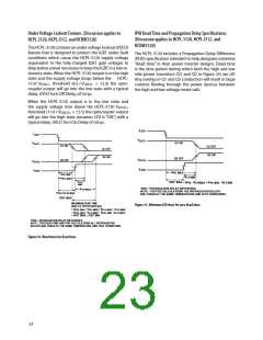
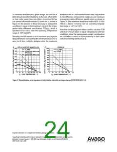
Qg = 100 nC
Qg = 500 nC
Qg = 1000 nC
+ꢀP •(———————ꢀꢀ+ꢀq )ꢀ+ꢀT
A
D
CA
ꢀ ꢀ ꢀꢀꢀ q ꢀ+ꢀq ꢀ+ꢀq
LD
LC
DC
V
V
= 19 V
= -9 V
CC
EE
ꢀ ꢀ ꢀ ꢀ ꢀ q ꢀ•ꢀq
LC
DC
8
6
4
3
T ꢀ= P ꢀ(———————ꢀꢀ+ꢀq
)
CA
JD ꢀ E
ꢀ ꢀ ꢀ ꢀꢀ ꢀ q ꢀ+ꢀq ꢀ+ꢀq
LD
LC
DC
+ꢀP • (q ||(q ꢀ+ꢀq )ꢀ+ꢀq )ꢀ+ꢀT
A
Dꢀ
DC LD
LC
CA
Insertingꢀtheꢀvaluesꢀforꢀq ꢀandꢀq ꢀshownꢀinꢀFigureꢀ28ꢀ
gives:
LC
DC
0
0
10
30
ꢀ0
40
50
Rg – GATE RESISTANCE – Ω
T ꢀ=ꢀP • (256°C/Wꢀ+ꢀq )ꢀ
JE
Eꢀ
CA
ꢀ ꢀꢀ+ꢀP • (57°C/Wꢀ+ꢀq )ꢀ+ꢀT
Dꢀ
CA
Aꢀ
T ꢀ=ꢀP • (57°C/Wꢀ+ꢀq )ꢀ
JD
Eꢀ
CA
Figure 27. Energy dissipated in the HCPL-3120 for each IGBT switching
cycle.
ꢀ ꢀꢀ+ꢀP • (111°C/Wꢀ+ꢀq )ꢀ+ꢀT
A
Dꢀ
CA
Forꢀexample,ꢀgivenꢀP ꢀ=ꢀ45ꢀmW,ꢀP ꢀ=ꢀ250ꢀmW,ꢀT ꢀ=ꢀ70°Cꢀ
E
O
A
andꢀ q ꢀ=ꢀ83°C/W:
CA
TJEꢀ=ꢀPEꢀ• 339°C/Wꢀ+ꢀPDꢀ• 140°C/Wꢀ+ꢀTAꢀ
ꢀ ꢀꢀ=ꢀ45ꢀmWꢀ• 339°C/Wꢀ+ꢀ250ꢀmWꢀ
ꢀ
ꢀ ꢀ ꢀ
• 140°C/Wꢀ+ꢀ70°Cꢀ=ꢀ120°C
TJDꢀ=ꢀPEꢀ• 140°C/Wꢀ+ꢀPDꢀ• 194°C/Wꢀ+ꢀTAꢀ
ꢀ ꢀꢀ=ꢀ45ꢀmWꢀ• 140°C/Wꢀ+ꢀ250ꢀmWꢀ• 194°C/Wꢀ+ꢀ70°Cꢀ=ꢀ125°C
T ꢀ andꢀ T ꢀ shouldꢀ beꢀ limitedꢀ toꢀ 125°Cꢀ basedꢀ onꢀ theꢀ
JE
JD
boardꢀlayoutꢀandꢀpartꢀplacementꢀ(q )ꢀspecificꢀtoꢀtheꢀap-
CA
plication.
20

 AVAGO [ AVAGO TECHNOLOGIES LIMITED ]