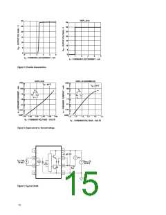
TheꢀV ꢀvalueꢀofꢀ2Vꢀinꢀtheꢀpreviousꢀequationꢀisꢀaꢀcon-
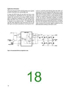
Selectingꢀ theꢀ Gateꢀ Resistorꢀ (Rg)ꢀ toꢀ Minimizeꢀ IGBTꢀ Forꢀ theꢀ circuitꢀ inꢀ Figureꢀ 26ꢀ withꢀ I ꢀ (worstꢀ case)ꢀ =ꢀ
F
Switchingꢀ Losses.ꢀ (Discussionꢀ appliesꢀ toꢀ HCPL-3120,ꢀ 16ꢀmA,ꢀRgꢀ=ꢀ8ꢀΩ,ꢀMaxꢀDutyꢀCycleꢀ=ꢀ80%,ꢀQgꢀ=ꢀ500ꢀnC,ꢀ
HCPL-J312ꢀandꢀHCNW3120)
fꢀ=ꢀ20ꢀkHzꢀandꢀT ꢀmaxꢀ=ꢀ85ꢀ°C:
A
Stepꢀ1:ꢀCalculateꢀRgꢀMinimumꢀfromꢀtheꢀI ꢀPeakꢀSpecifica- P ꢀ=ꢀ16ꢀmAꢀ• 1.8ꢀVꢀ• 0.8ꢀ=ꢀ23ꢀmW
OL
E
tion.ꢀTheꢀIGBTꢀandꢀRgꢀinꢀFigureꢀ26ꢀcanꢀbeꢀanalyzedꢀasꢀaꢀ
simpleꢀRCꢀcircuitꢀwithꢀaꢀvoltageꢀsuppliedꢀbyꢀtheꢀHCPL-
3120.
P ꢀ=ꢀ4.25ꢀmAꢀ• 20ꢀVꢀ+ꢀ5.2ꢀµꢀJꢀ• 20ꢀkHz
O
ꢀ ꢀ=ꢀ85ꢀmWꢀ+ꢀ104ꢀmW
ꢀ
ꢀ
ꢀ
(V ꢀ–ꢀV ꢀ-ꢀV )ꢀ
ꢀ ꢀ=ꢀ189ꢀmWꢀ>ꢀ178ꢀmWꢀ(P
ꢀ@ꢀ85°C
CC
EE
OL
O(MAX)
Rgꢀ ≥ꢀ ———————ꢀꢀ
ꢀ
ꢀ
ꢀ
ꢀ
ꢀ ꢀ I
OLPEAKꢀ
ꢀ ꢀ=ꢀ250ꢀmW-15C*4.8ꢀmW/C)
ꢀ
(V ꢀ–ꢀV ꢀ-ꢀ2ꢀV)ꢀ
ꢀ
ꢀ
ꢀ
CC
EE
ꢀ
=ꢀ ———————ꢀꢀ
ꢀ
ꢀ
ꢀ ꢀ
Theꢀvalueꢀofꢀ4.25ꢀmAꢀforꢀI ꢀinꢀtheꢀpreviousꢀequationꢀwasꢀ
CC
ꢀ
ꢀ
ꢀ
ꢀ
ꢀ
ꢀꢀꢀꢀꢀ I
OLPEAKꢀ
obtainedꢀbyꢀderatingꢀtheꢀI ꢀmaxꢀofꢀ5ꢀmAꢀ(whichꢀoccursꢀ
CC
ꢀ
(15ꢀVꢀ+ꢀ5ꢀVꢀ-ꢀ2ꢀV)ꢀ
atꢀ-40°C)ꢀtoꢀI ꢀmaxꢀatꢀ85Cꢀ(seeꢀFigureꢀ7).
CC
=ꢀ ———————ꢀꢀ
ꢀ
ꢀ
ꢀ
ꢀ ꢀ ꢀꢀꢀ
ꢀ
ꢀꢀꢀ2.5ꢀAꢀ
ꢀ
ꢀ
SinceꢀP ꢀforꢀthisꢀcaseꢀisꢀgreaterꢀthanꢀP
,ꢀRgꢀmustꢀbeꢀ
O(MAX)
O
ꢀ
=ꢀ 7.2ꢀΩꢀ@ꢀ8ꢀΩ
ꢀ
increasedꢀtoꢀreduceꢀtheꢀHCPL-3120ꢀpowerꢀdissipation.
OL
P
ꢀ ꢀ
O(SWITCHINGꢀMAX)
servativeꢀvalueꢀofꢀV ꢀatꢀtheꢀpeakꢀcurrentꢀofꢀ2.5Aꢀ(seeꢀ
OL
Figureꢀ6).ꢀAtꢀlowerꢀRgꢀvaluesꢀtheꢀvoltageꢀsuppliedꢀbyꢀ
theꢀHCPL-3120ꢀisꢀnotꢀanꢀidealꢀvoltageꢀstep.ꢀThisꢀresultsꢀ
inꢀlowerꢀpeakꢀcurrentsꢀ(moreꢀmargin)ꢀthanꢀpredictedꢀbyꢀ
ꢀ
=ꢀP
ꢀ-ꢀP
O(MAX) O(BIAS)
ꢀ ꢀ=ꢀ178ꢀmWꢀ-ꢀ85ꢀmW
ꢀ
=ꢀ93ꢀmW
thisꢀanalysis.ꢀWhenꢀnegativeꢀgateꢀdriveꢀisꢀnotꢀusedꢀV ꢀinꢀ
EE
ꢀ
theꢀpreviousꢀequationꢀisꢀequalꢀtoꢀzeroꢀvolts.
ꢀ ꢀ
ꢀ
ꢀ
ꢀP
ꢀ
O(SWITCHINGMAX)
E
ꢀ
=ꢀ ———————ꢀ
SW(MAX)
ꢀ ꢀ
ꢀ ꢀ ꢀ ꢀfꢀ
Stepꢀ2:ꢀCheckꢀtheꢀHCPL-3120ꢀPowerꢀDissipationꢀandꢀ
IncreaseꢀRgꢀifꢀNecessary.ꢀTheꢀHCPL-3120ꢀtotalꢀpowerꢀ
ꢀ
ꢀ
ꢀ ꢀ
ꢀ
93ꢀmWꢀ
ꢀ ꢀ
=ꢀꢀ————ꢀ=ꢀ4.65ꢀµWꢀ
dissipationꢀ(P )ꢀisꢀequalꢀtoꢀtheꢀsumꢀofꢀtheꢀemitterꢀpowerꢀ
T
20ꢀkHz
ꢀ ꢀ
ꢀ ꢀ
(P )ꢀandꢀtheꢀoutputꢀpowerꢀ(P ):
E
O
P ꢀ=ꢀP ꢀ+ꢀP
O
T
E
ForꢀQgꢀ=ꢀ500ꢀnC,ꢀfromꢀFigureꢀ27,ꢀaꢀvalueꢀofꢀE ꢀ=ꢀ4.65ꢀµWꢀ
givesꢀaꢀꢀꢀRgꢀ=ꢀ10.3ꢀΩ.
SW
PEꢀ=ꢀI •ꢀV ·ꢀDutyꢀCycle
Fꢀ Fꢀ
P ꢀ=ꢀP
ꢀ+ꢀP
O(BIAS) Oꢀ(SWITCHING)
O
ꢀ ꢀ =ꢀI ꢀ•ꢀ(V ꢀ-ꢀV )+ꢀE (R ,ꢀQ )ꢀ•ꢀf
CC
CC
EE
SW
G
G
HCPL-ꢀ130
+5 V
1
8
V
= 15 V
CC
+ HVDC
370 Ω
0.1 µF
+
–
3
ꢀ
4
7
6
5
Rg
Q1
= -5 V
ꢀ-PHASE
AC
CONTROL
INPUT
V
EE
+
–
74XXX
OPEN
COLLECTOR
Q3
- HVDC
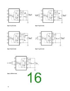
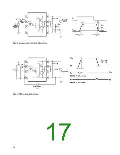
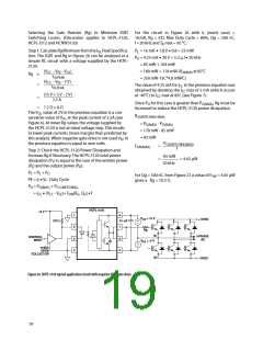
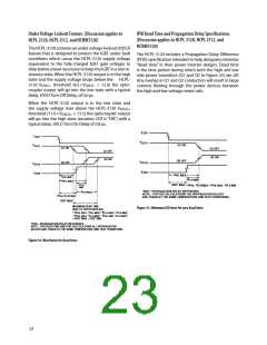
Figure 26. HCPL-3120 typical application circuit with negative IGBT gate drive.
19

 AVAGO [ AVAGO TECHNOLOGIES LIMITED ]