VRAM
SMJ44C251B
MT42C4256
Austin Semiconductor, Inc.
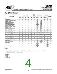
FUNCTION TABLE
CAS\
FALL
RAS\ FALL
ADDRESS
RAS\ CAS\
DQ0 - DQ3
TYPE3
FUNCTION
CAS\2
W\1
X
CAS\ TRG\
DSF
SE\
DSF
RAS\
W\
CBR Refresh
Register-to-memory transfer
(transfer write)
L
X
L
X
X
X
L
X
X
X
Row
Addr
Row
Addr
Refresh
Addr
Row
Addr
Row
Addr
Row
Addr
X
X
X
X
R
T
Tap
Point
Tap
Point
Tap
Point
Tap
Point
Tap
Point
Col
H
L
X
X
X
X
Alternate transfer write
(independent of SE\)
Serial-write-mode enable
(pseudo-transfer write)
Memory-to-register transfer
(transfer read)
H
H
H
H
H
H
H
H
H
H
H
H
L
L
L
L
H
L
X
H
X
X
X
X
X
X
X
X
X
X
X
X
X
X
L
X
X
X
T
T
L
H
H
L
L
T
Split-register-transfer read
(must reload tap)
L
H
L
X
X
T
Load and use write mask,
Write data to DRAM
Load and use write mask,
Block write to DRAM
Persistent write-per-bit,
Write data to DRAM
Persistent write-per-bit,
Block write to DRAM
Normal DRAM read/write
(nonmasked)
DQ
Valid
L
R
R
R
R
R
R
R
R
Addr
Row Blk Addr
Mask Data
DQ Col
Mask Mask
H
H
H
H
H
H
H
L
L
H
L
Addr
Row
Addr
A2-A8
Col
Addr
Valid
Data
L
H
H
L
X
Row Blk Addr
Col
Mask
L
H
L
X
Addr
Row
Addr
A2-A8
Col
Addr
Valid
Data
H
H
H
H
X
Block write to DRAM
(nonmasked)
Row Blk Addr
Col
Mask
L
H
L
X
Addr
Refresh
Addr
Refresh
Addr
A2-A8
DQ
Mask
Load write mask
H
H
X
X
Color
Data
Load color register
H
X
X
NOTES:
1. In persistent write-per-bit function, W\ must be high during the refresh cycle.
2. DQ0 - DQ3 are latched on the later of W\ or CAS\ falling edge. Col Mask = H: Write to address/column location enabled.
DQ Mask = H: Write to I/O enabled.
3. R = random access operation, T = transfer operation.
LEGEND
H = HIGH
L = LOW
X = Don’t Care
Austin Semiconductor, Inc. reserves the right to change products or specifications without notice.
SMJ44C251B/MT42C4256
Rev. 0.1 12/03
4

 AUSTIN [ AUSTIN SEMICONDUCTOR ]