VRAM
SMJ44C251B
MT42C4256
Austin Semiconductor, Inc.
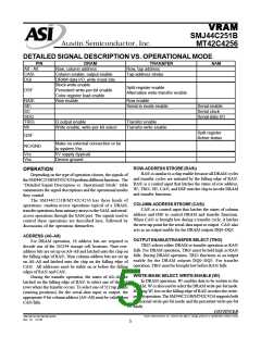
DETAILED SIGNAL DESCRIPTION VS. OPERATIONAL MODE
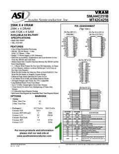
PIN
A0 - A8
DRAM
Row, column address
TRANSFER
Row, tap address
SAM
CAS\
DQi
Column enable, output enable
DRAM data I/O, write mask bits
Block-write enable
Persistent write-per-bit enable
Color-register load enable
Row enable
Tap-address strobe
Split-register enable
Alternative write-transfer enable
DSF
RAS\
SE\
Row enable
Serial-in mode enable
Serial enable
Serial clock
SC
SDQ
TRG\
W\
Serial-data I/O
Q output enable
Write enable, write-per-bit select
Transfer enable
Transfer-write enable
Split register
Active status
QSF
Make no external connection or tie
to system Vss
NC/GND
Vcc
Vss
5V supply (typical)
Device ground
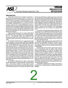
ROW-ADDRESS STROBE (RAS\)
OPERATION
RAS\ is similar to a chip enable because all DRAM cycles
and transfer cycles are initiated by the falling edge of RAS\.
RAS\ is a control input that latches the states of row address,
W\, TRG\, SE\, CAS\, and DSF onto the chip to invoke DRAM
and transfer functions.
Depending on the type of operation chosen, the signals of
the SMJ44C251B/MT42C4256 perform different functions. The
“Detailed Signal Description vs. Operational Mode” table
summarizes the signal descriptions and the operational modes
they control.
The SMJ44C251B/MT42C4256 has three kinds of
operations: random-access operations typical of a DRAM,
transfer operations from memory arrays to the SAM, and serial-
access operations through the SAM port. The signals used to
control these operations are described here, followed by
discussions of the operations themselves.
COLUMN-ADDRESS STROBE (CAS\)
CAS\ is a control input that latches the states of column
address and DSF to control DRAM and transfer functions.
When CAS\ is brought low during a transfer cycle, it latches
the new tap point for the serial-data input or output. CAS\ also
acts as an output enable for the DRAM outputs DQ0–DQ3.
ADDRESS (A0–A8)
OUTPUT ENABLE/TRANSFER SELECT (TRG\)
For DRAM operation, 18 address bits are required to
decode one of the 262144 storage cell locations. Nine row-
address bits are set up on A0–A8 and latched onto the chip on
the falling edge of RAS\. Nine column-address bits are set up
on A0–A8 and latched onto the chip on the falling edge of
CAS\. All addresses must be stable on or before the falling
edges of RAS\ and CAS\.
TRG\ selects either DRAM or transfer operation as RAS\
falls. For DRAM operation, TRG\ must be held high as RAS\
falls. During DRAM operation, TRG\ functions as an output
enable for the DRAM outputs DQ0–DQ3. For transfer
operation, TRG\ must be brought low before RAS\ falls.
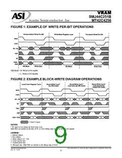
WRITE-MASK SELECT, WRITE ENABLE (W\)
In DRAM operation, W\ enables data to be written to the
DRAM. W\ is also used to select the DRAM write-per-bit mode.
Holding W\ low on the falling edge of RAS\ invokes the write-
per-bit operation. The SMJ44C251B/MT42C4256 supports both
the normal write-per-bit mode and the persistent write-per-bit
mode.
During the transfer operation, the states of A0–A8 are
latched on the falling edge of RAS\ to select one of the 512
rows where the transfer occurs. To select one of 512 tap points
(starting positions) for the serial-data input or output, the
appropriate 9-bit column address (A0–A8) must be valid when
CAS\ falls.
CONTINUED
Austin Semiconductor, Inc. reserves the right to change products or specifications without notice.
SMJ44C251B/MT42C4256
Rev. 0.1 12/03
5

 AUSTIN [ AUSTIN SEMICONDUCTOR ]