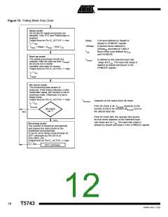
T5743
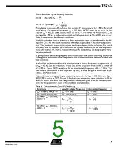
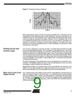
Figure 8. Receiving Frequency Response
0.0
-10.0
-20.0
-30.0
-40.0
-50.0
-60.0
-70.0
-80.0
-90.0
without SAW
with SAW
-100.0
-6.0 -5.0 -4.0 -3.0 -2.0 -1.0 0.0
1.0 2.0 3.0 4.0 5.0 6.0
df (MHz)
When designing the system in terms of receiving bandwidth, the LO deviation must be
considered as it also determines the IF center frequency. The total LO deviation is cal-
culated to be the sum of the deviation of the crystal and the XTO deviation of the T5743.
Low-cost crystals are specified to be within ±100 ppm. The XTO deviation of the T5743
is an additional deviation due to the XTO circuit. This deviation is specified to be
±30 ppm. If a crystal of ±100 ppm is used, the total deviation is ±130 ppm in that case.
Note that the receiving bandwidth and the IF-filter bandwidth are equivalent in ASK
mode but not in FSK mode.
Polling Circuit and
Control Logic
The receiver is designed to consume less than 1 mA while being sensitive to signals
from a corresponding transmitter. This is achieved via the polling circuit. This circuit
enables the signal path periodically for a short time. During this time the bit-check logic
verifies the presence of a valid transmitter signal. Only if a valid signal is detected the
receiver remains active and transfers the data to the connected microcontroller. If there
is no valid signal present the receiver is in sleep mode most of the time resulting in low
current consumption. This condition is called polling mode. A connected microcontroller
is disabled during that time.
All relevant parameters of the polling logic can be configured by the connected micro-
controller. This flexibility enables the user to meet the specifications in terms of current
consumption, system response time, data rate etc.
Regarding the number of connection wires to the microcontroller, the receiver is very
flexible. It can be either operated by a single bi-directional line to save ports to the con-
nected microcontroller or it can be operated by up to five uni-directional ports.
Basic Clock Cycle of the The complete timing of the digital circuitry and the analog filtering is derived from one
clock. According to Figure 9, this clock cycle TClk is derived from the crystal oscillator
Digital Circuitry
(XTO) in combination with a divider. The division factor is controlled by the logical state
at Pin MODE. According to section “RF Front-end”, the frequency of the crystal oscillator
(fXTO) is defined by the RF input signal (fRFin) which also defines the operating frequency
of the local oscillator (fLO).
9
4569A–RKE–12/02

 ATMEL [ ATMEL ]