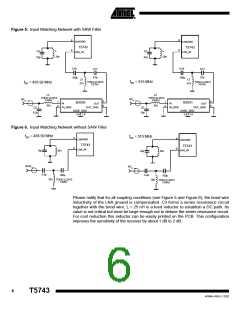
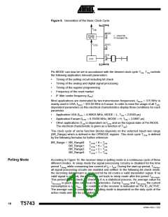
Figure 9. Generation of the Basic Clock Cycle
T
Clk
MODE
Divider
L : USA(:10)
16
H: Europe(:14)
:14/:10
f
DVCC
15
XTO
XTO
14
XTO
Pin MODE can now be set in accordance with the desired clock cycle TClk. TClk controls
the following application relevant parameters:
•
•
•
•
•
Timing of the polling circuit including bit check
Timing of the analog and digital signal processing
Timing of the register programming
Frequency of the reset marker
IF filter center frequency (fIF0
)
Most applications are dominated by two transmission frequencies: fSend = 315 MHz is
mainly used in USA, fSend = 433.92 MHz in Europe. In order to ease the usage of all TClk
-
dependent parameters on this electrical characteristics display three conditions for each
parameter.
•
•
•
Application USA (fXTO = 4.90625 MHz, MODE = L, TClk = 2.0383 µs)
Application Europe (fXTO = 6.76438 MHz, MODE = H, TClk = 2.0697 µs)
Other applications (TClk is dependent on fXTO and on the logical state of Pin MODE.
The electrical characteristic is given as a function of TClk).
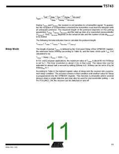
The clock cycle of some function blocks depends on the selected baud-rate range
(BR_Range) which is defined in the OPMODE register. This clock cycle TXClk is defined
by the following formulas for further reference:
BR_Range = BR_Range0:
TXClk = 8 P TClk
BR_Range1: TXClk = 4 P TClk
BR_Range2: TXClk = 2 P TClk
BR_Range3: TXClk = 1 P TClk
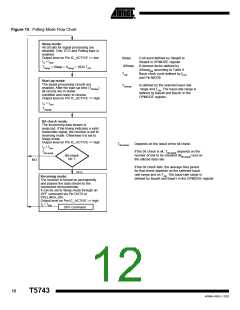
Polling Mode
According to Figure 10, the receiver stays in polling mode in a continuous cycle of three
different modes. In sleep mode the signal processing circuitry is disabled for the time
period TSleep while consuming low current of IS = ISoff. During the start-up period, TStartup
,
all signal processing circuits are enabled and settled. In the following bit-check mode,
the incoming data stream is analyzed bit by bit contra a valid transmitter signal. If no
valid signal is present, the receiver is set back to sleep mode after the period TBit-check
This period varies check by check as it is a statistical process. An average value for
Bit-check is given in the electrical characteristics. During TStartup and TBit-check the current
.
T
consumption is IS = ISon. The condition of the receiver is indicated on Pin IC_ACTIVE.
The average current consumption in polling mode is dependent on the duty cycle of the
active mode and can be calculated as:
10
T5743
4569A–RKE–12/02

 ATMEL [ ATMEL ]