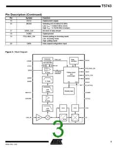
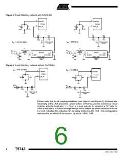
Figure 5. Input Matching Network with SAW Filter
8
8
9
LNAGND
LNAGND
T5743
T5743
9
L
L
C3
C3
LNA_IN
LNA_IN
25n
25n
22p
47p
C16
C16
C17
8.2p
C17
22p
100p
100p
L3
L3
TOKO LL2012
F27NJ
fRF = 315 MHz
TOKO LL2012
F47NJ
fRF = 433.92 MHz
27n
47n
L2
L2
TOKO LL2012
TOKO LL2012
F82NJ
RFIN
RFIN
F33NJ
5
5
1
2
1
B3555
B3551
IN
IN
OUT
OUT
33n
82n
6
6
2
OUT_GND
OUT_GND
IN_GND
IN_GND
C2
C2
CASE_GND
3,4 7,8
CASE_GND
3,4 7,8
8.2p
10p
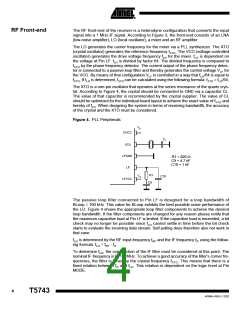
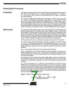
Figure 6. Input Matching Network without SAW Filter
fRF = 433.92 MHz
fRF = 315 MHz
8
8
9
LNAGND
LNAGND
T5743
T5743
LNA_IN
9
LNA_IN
25n
15p
25n
33p
RFIN
RFIN
3.3p
100p
3.3p
100p
22n
TOKO LL2012
F22NJ
39n
TOKO LL2012
F39NJ
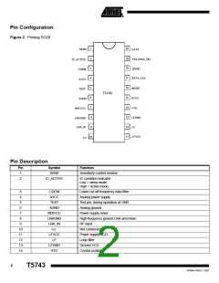
Please notify that for all coupling conditions (see Figure 5 and Figure 6), the bond wire
inductivity of the LNA ground is compensated. C3 forms a series resonance circuit
together with the bond wire. L = 25 nH is a feed inductor to establish a DC path. Its
value is not critical but must be large enough not to detune the series resonance circuit.
For cost reduction this inductor can be easily printed on the PCB. This configuration
improves the sensitivity of the receiver by about 1 dB to 2 dB.
6
T5743
4569A–RKE–12/02

 ATMEL [ ATMEL ]