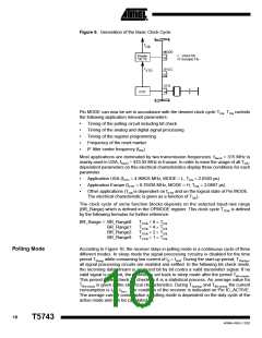
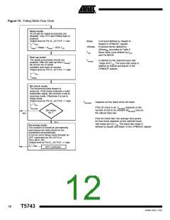
Figure 10. Polling Mode Flow Chart
Sleep mode:
All circuits for signal processing are
disabled. Only XTO and Polling logic is
enabled.
Output level on Pin IC_ACTIVE => low
IS = ISoff
Sleep:
Sleep:
5-bit word defined by Sleep0 to
5-bit word defined by Sleep0 to
Sleep4 in OPMODE register
Sleep4 in OPMODE register
XSleep: Extension factor defined by
XSleep: Extension factor defined by
TSleep = Sleep P X
P
P 1024 T
Clk
Clk
P
Sleep
l
XSleep according to Table 9
XSleepStd according to Table 9
T
:
Basic cSlotdck cycle defined by f
T
:
Basic clock cycle defined by f
Clk
Clk
XTO
XTO
and Pin MODE
and Pin MODE
Start-up mode:
The signal processing circuits are
enabled. After the start-up time (TStartup
all circuits are in stable
condition and ready to receive.
Output level on Pin IC_ACTIVE => high
T
:
Is defined by the selected baud rate
Is defined by the selected baud rate
T
:
Startup
Startup
)
)
Startup
range and T . The baud-rate range is
Clk. The baud-rate range is
Clk
defined by Baud0 and Baud1 in the
defined by Baud0 and Baud1 in the
OPMODE register.
OPMODE register.
IS = ISon
TStartup
Bit-check mode:
The incomming data stream is
analyzed. If the timing indicates a valid
transmitter signal, the receiver is set to
receiving mode. Otherwise it is set to
Sleep mode.
Output level on Pin IC_ACTIVE => high
T
:
Depends on the result of the bit check.
Depends on the result of the bit check.
TBit-check
:
Bit-check
IS = ISon
S
Son
If the bit check is ok, T
depends on the
If the bit check is ok, TBit-check depends on the
TBit-check
Bit-check
Bit-check
number of bits to be checked (N
) and on
Bit-check
OK ?
number of bits to be checked (NBit-check ) and on
Bit-check
the utilized data rate.
the utilized data rate.
NO
If the bit check fails, the average time period
If the bit check fails, the average time period
for that check depends on the selected baud-
for that check depends on the selected baud-
YES
rate range and on T . The baud-rate range is
rate range and on TClk . The baud-rate range is
Clk
Receiving mode:
The receiver is turned on permanently
and passes the data stream to the
defined by Baud0 and Baud1 in the OPMODE register
defined by Baud0 and Baud1 in the OPMODE register
connected microcontroller.
C.
It can be set to Sleep mode through an
OFF command via Pin DATA or
POLLING/_ON.
Output level on Pin IC_ACTIVE => high
Output level on Pin IC_ACTIVE => high
I = I
IS = ISon
S
Son
OFF command
OFF command
12
T5743
4569A–RKE–12/02

 ATMEL [ ATMEL ]