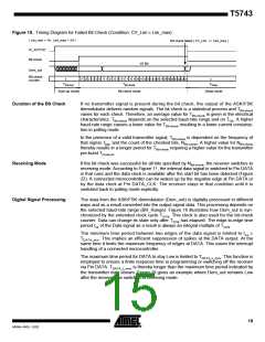
Figure 21. Activating the Receiving Mode via Pin POLLING/_ON
IC_ACTIVE
ton1
POLLING/_ON
X
Data_out (DATA)
Serial bi-directional
data line
X
Sleep mode
Start-up mode
Receiving mode
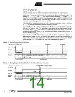
Figure 20 illustrates how to set the receiver back to polling mode via Pin POLLING/_ON.
The Pin POLLING/_ON must be held to low for the time period ton2. After the positive
edge on Pin POLLING/_ON and the delay ton3, the polling mode is active and the sleep
time TSleep elapses.
This command is faster than using Pin DATA at the cost of an additional connection to
the microcontroller.
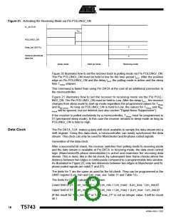
Figure 21 illustrates how to set the receiver to receiving mode via the Pin POLL-
ING/_ON. The Pin POLLING/_ON must be held to Low. After the delay ton1 , the receiver
changes from sleep mode to start-up mode regardless the programmed values for TSleep
and NBit-check. As long as POLLING/_ON is held to Low, the values for TSleep and NBit-
check will be ignored, but not deleted (see also section “Digital Noise Suppression”).
If the receiver is polled exclusively by a microcontroller, TSleep must be programmed to
31 (permanent sleep mode). In this case the receiver remains in sleep mode as long as
POLLING/_ON is held to High.
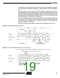
Data Clock
The Pin DATA_CLK makes a data shift clock available to sample the data stream into a
shift register. Using this data clock, a microcontroller can easily synchronize the data
stream. This clock can only be used for Manchester and Bi-phase coded signals.
Generation of the data clock:
After a successful bit check, the receiver switches from polling mode to receiving mode
and the data stream is available at Pin DATA. In receiving mode, the data clock control
logic (Manchester/Bi-phase demodulator) is active and examines the incoming data
stream. This is done, like in the bit check, by subsequent time frame checks where the
distance between two edges is continuously compared to a programmable time window.
As illustrated in Figure 22, only two distances between two edges in Manchester and Bi-
phase coded signals are valid (T and 2T).
The limits for T are the same as used for the bit check. They can be programmed in the
LIMIT-register (Lim_min and Lim_max, see Table 11 and Table 12).
The limits for 2T are calculated as follows:
Lower limit of 2T: Lim_min_2T =
Upper limit of 2T: Lim_max_2T=
(Lim_min + Lim_max) - (Lim_max - Lim_min)/2
(Lim_min + Lim_max) + (Lim_max - Lim_min)/2
(If the result for “Lim_min_2T” or “Lim_max_2T” is not an integer value, it will be round
up.)
18
T5743
4569A–RKE–12/02

 ATMEL [ ATMEL ]