T5743
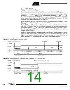
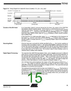
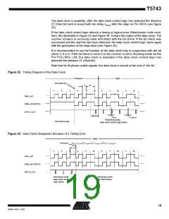
Figure 15. Timing Diagram for Failed Bit Check (Condition: CV_Lim O Lim_max)
( Lim_min = 14, Lim_max = 24 )
Bit check failed ( CV_Lim >= Lim_max )
IC_ACTIVE
Bit check
1/2 Bit
Dem_out
Bit-check-
1
2
3
4
5
6
1
2
3
4
5
6
7
8
9
10 11 12 13 14 15 16
18 19 20 21 22 23 24
17
0
7
0
counter
TStart-up
TBit-check
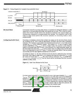
Bit-check mode
TSleep
Start-up mode
Sleep mode
Duration of the Bit Check
If no transmitter signal is present during the bit check, the output of the ASK/FSK
demodulator delivers random signals. The bit check is a statistical process and TBit-check
varies for each check. Therefore, an average value for TBit-check is given in the electrical
characteristics. TBit-check depends on the selected baud-rate range and on TClk. A higher
baud-rate range causes a lower value for TBit-check resulting in a lower current consump-
tion in polling mode.
In the presence of a valid transmitter signal, TBit-check is dependent on the frequency of
that signal, fSig, and the count of the checked bits, NBit-check. A higher value for NBit-check
thereby results in a longer period for TBit-check requiring a higher value for the transmitter
pre-burst TPreburst
.
Receiving Mode
If the bit check was successful for all bits specified by NBit-check, the receiver switches to
receiving mode. According to Figure 11, the internal data signal is switched to Pin DATA
in that case and the data clock is available after the start bit has been detected (Figure
22). A connected microcontroller can be woken up by the negative edge at Pin DATA or
by the data clock at Pin DATA_CLK. The receiver stays in that condition until it is
switched back to polling mode explicitly.
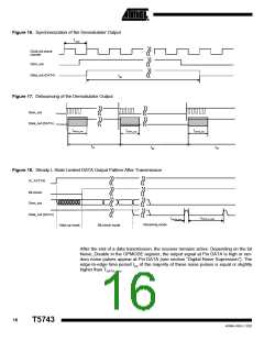
Digital Signal Processing
The data from the ASK/FSK demodulator (Dem_out) is digitally processed in different
ways and as a result converted into the output signal data. This processing depends on
the selected baud-rate range (BR_Range). Figure 16 illustrates how Dem_out is syn-
chronized by the extended clock cycle TXClk. This clock is also used for the bit-check
counter. Data can change its state only after TXClk has elapsed. The edge-to-edge time
period tee of the Data signal as a result is always an integral multiple of TXClk
The minimum time period between two edges of the data signal is limited to tee
DATA_min. This implies an efficient suppression of spikes at the DATA output. At the
.
O
T
same time it limits the maximum frequency of edges at DATA. This eases the interrupt
handling of a connected microcontroller.
The maximum time period for DATA to stay Low is limited to TDATA_L_max. This function is
employed to ensure a finite response time in programming or switching off the receiver
via Pin DATA. TDATA_L_max is thereby longer than the maximum time period indicated by
the transmitter data stream. Figure 18 gives an example where Dem_out remains Low
after the receiver has switched to receiving mode.
15
4569A–RKE–12/02

 ATMEL [ ATMEL ]