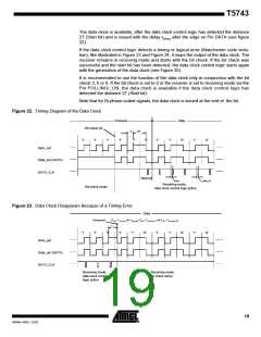
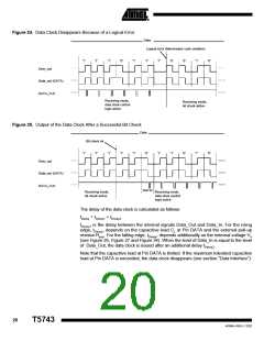
Figure 24. Data Clock Disappears Because of a Logical Error
Data
Logical error (Manchester code violation)
'1'
'1'
'1'
'0'
'1'
'1'
'?'
'0'
'0'
'1'
'0'
Dem_out
Data_out (DATA)
DATA_CLK
Receiving mode,
data clock control
logic active
Receiving mode,
bit check aktive
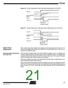
Figure 25. Output of the Data Clock After a Successful Bit Check
Data
Bit check ok
'1'
'1'
'1'
'1'
'1'
'0'
'1'
'1'
'0'
'1'
'0'
Dem_out
Data_out (DATA)
DATA_CLK
Start bit
Receiving mode,
bit check active
Receiving mode,
data clock control
logic active
The delay of the data clock is calculated as follows:
Delay = tDelay1 + tDelay2
t
tDelay1 is the delay between the internal signals Data_Out and Data_In. For the rising
edge, tDelay1 depends on the capacitive load CL at Pin DATA and the external pull-up
resistor Rpup. For the falling edge, tDelay1 depends additionally on the external voltage VX
(see Figure 26, Figure 27 and Figure 34). When the level of Data_In is equal to the level
of Data_Out, the data clock is issued after an additional delay tDelay2
.
Note that the capacitive load at Pin DATA is limited. If the maximum tolerated capacitive
load at Pin DATA is exceeded, the data clock disappears (see section “Data Interface”).
20
T5743
4569A–RKE–12/02

 ATMEL [ ATMEL ]