T5743
Switching the Receiver Back
to Sleep Mode
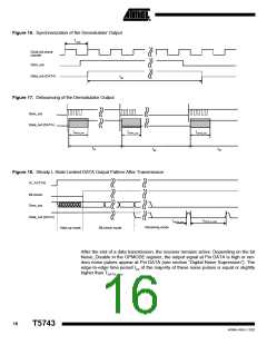
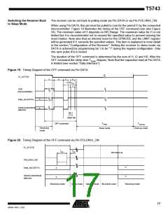
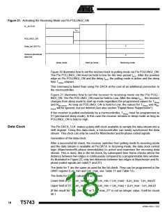
The receiver can be set back to polling mode via Pin DATA or via Pin POLLING/_ON.
When using Pin DATA, this pin must be pulled to Low for the period t1 by the connected
microcontroller. Figure 19 illustrates the timing of the OFF command (see also Figure
34). The minimum value of t1 depends on BR_Range. The maximum value for t1 is not
limited but it is recommended not to exceed the specified value to prevent erasing the
reset marker. Note also that an internal reset for the OPMODE and the LIMIT register
will be generated if t1 exceeds the specified values. This item is explained in more detail
in the section “Configuration of the Receiver”. Setting the receiver to sleep mode via
DATA is achieved by programming bit 1 to be “1” during the register configuration. Only
one sync pulse (t3) is issued.
The duration of the OFF command is determined by the sum of t1, t2 and t10. After the
OFF command the sleep time TSleep elapses. Note that the capacitive load at Pin DATA
is limited (see section “Data Interface”).
Figure 19. Timing Diagram of the OFF-command via Pin DATA
IICC___AACCCTTTIIIVVVEEE
IC_ACTIVE
t1
tt11
t2
tt22
t3
tt33
t5
tt55
t1
t2
t3
t5
t4
tt44
t4
t10
tt1100
t10
t7
tt77
t7
Out1
Out1
Out1
Out1 (mC)
(microcontroller)
(microcontroller)
(microcontroller
X
X
Data_out (DATA)
DDaattaa__oouutt ((DDAATTAA))
X
Data_out (DATA)
Serial bi-directional
Serial bi-directional
Serial bi-directional
X
X
Serial bi-directional
X
data line
data line
data line
data line
Bit 1
Bit 1
Bit 1
Bit 1
("1")
("1")
("1")
("1")
(Start bit)
(Start bit)
(Start bit)
(Start bit)
T
OFF-command
TT
Sleep
Sleep
OOFFFF--ccoommmmaanndd
T
TT
Start-up
SStatartr-tu-upp
TSleep
OFF-command
TStart-up
Sleep
Receiving
Receiving
Sleep mode
Start-up mode
Receiving
Sleep mode
Sleep mode
Start-up mode
Start-up mode
Receiving
Sleep mode
Start-up mode
mode
mode
mode
mode
Figure 20. Timing Diagram of the OFF-command via Pin POLLING/_ON
IC_ACTIVE
ton2
ton3
Bit check ok
POLLING/_ON
X
X
Data_out (DATA)
X
X
Serial bi-directional
data line
Receiving mode
Sleep mode
Start-up mode Bit-check mode
Receiving mode
17
4569A–RKE–12/02

 ATMEL [ ATMEL ]