TLim_min = Lim_min P TXClk
TLim_max = (Lim_max –1) P TXClk
Lim_min and Lim_max are defined by a 5-bit word each within the LIMIT register.
Using above formulas, Lim_min and Lim_max can be determined according to the
required TLim_min, TLim_max and TXClk. The time resolution defining TLim_min and TLim_max is
T
XClk. The minimum edge-to-edge time tee (tDATA_L_min, tDATA_H_min) is defined according
to the section ‘Receiving Mode’. The lower limit should be set to Lim_min O 10. The
maximum value of the upper limit is Lim_max = 63.
If the calculated value for Lim_min is < 19, it is recommended to check 6 or 9 bits
(NBit-check) to prevent switching to receiving mode due to noise.
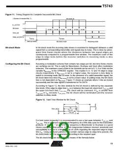
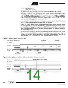
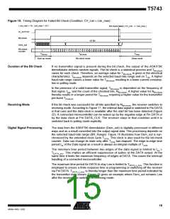
Figure 13, Figure 14 and Figure 15 illustrate the bit check for the bit-check limits
Lim_min = 14 and Lim_max = 24. When the IC is enabled, the signal processing circuits
are enabled during TStartup. The output of the ASK/FSK demodulator (Dem_out) is unde-
fined during that period. When the bit check becomes active, the bit-check counter is
clocked with the cycle TXClk
.
Figure 13 shows how the bit check proceeds if the bit-check counter value CV_Lim is
within the limits defined by Lim_min and Lim_max at the occurrence of a signal edge. In
Figure 14 the bit check fails as the value CV_lim is lower than the limit Lim_min. The bit
check also fails if CV_Lim reaches Lim_max. This is illustrated in Figure 15.
Figure 13. Timing Diagram During Bit Check
( Lim_min = 14, Lim_max = 24 )
IC_ACTIVE
Bit check ok
Bit check ok
Bit check
Dem_out
1/2 Bit
1/2 Bit
1/2 Bit
Bit-check-
1
2
3
4
5
6
7
8
1
2
3
4
5
6
7
8
9 10 11 12 13
14 15 16
17 18
1
2
3
4
5
6
7
8
9
10 11
12
13
14 15
1 2 3 4
0
counter
TXClk
TStart-up
TBit-check
Bit-check mode
Start-up mode
Figure 14. Timing Diagram for Failed Bit Check (Condition: CV_Lim < Lim_min)
( Lim_min = 14, Lim_max = 24 )
Bit check failed ( CV_Lim < Lim_min )
IC_ACTIVE
Bit check
1/2 Bit
Dem_out
Bit-check-
counter
1
2
3
4
5
6
1
2
4 5
3 6
7
8
9
10 11 12
0
0
TStart-up
TBit-check
Bit-check mode
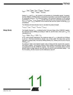
TSleep
Sleep mode
Start-up mode
14
T5743
4569A–RKE–12/02

 ATMEL [ ATMEL ]