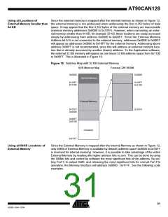
AT90CAN128
settings. This makes it possible to connect two different memory devices with different
timing requirements to the same XMEM interface. For XMEM interface timing details,
please refer to Tables 142 through Tables 149 and Figure 173 to Figure 176 in the
“External Data Memory Characteristics” on page 365.
Note that the XMEM interface is asynchronous and that the waveforms in the following
figures are related to the internal system clock. The skew between the internal and
external clock (XTAL1) is not guarantied (varies between devices temperature, and sup-
ply voltage). Consequently, the XMEM interface is not suited for synchronous operation.
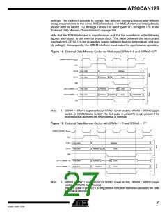
Figure 14. External Data Memory Cycles no Wait-state (SRWn1=0 and SRWn0=0)(1)
T1
T2
T3
T4
System Clock (CLKCPU
)
ALE
A15:8 Prev. addr.
DA7:0 Prev. data
WR
Address
Data
Address
XX
DA7:0 (XMBK = 0) Prev. data
DA7:0 (XMBK = 1) Prev. data
RD
Address
Address
Data
Data
XXXXX
XXXXXXXX
Note:
1. SRWn1 = SRW11 (upper sector) or SRW01 (lower sector), SRWn0 = SRW10 (upper
sector) or SRW00 (lower sector). The ALE pulse in period T4 is only present if the
next instruction accesses the RAM (internal or external).
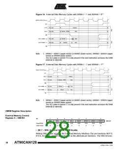
Figure 15. External Data Memory Cycles with SRWn1 = 0 and SRWn0 = 1(1)
T1
T2
T3
T4
T5
System Clock (CLKCPU
)
ALE
A15:8 Prev. addr.
DA7:0 Prev. data
WR
Address
Data
Address
Address
XX
DA7:0 (XMBK = 0) Prev. data
DA7:0 (XMBK = 1) Prev. data
RD
Data
Data
Address
Note:
1. SRWn1 = SRW11 (upper sector) or SRW01 (lower sector), SRWn0 = SRW10 (upper
sector) or SRW00 (lower sector).
The ALE pulse in period T5 is only present if the next instruction accesses the RAM
(internal or external).
27
4250E–CAN–12/04

 ATMEL [ ATMEL ]