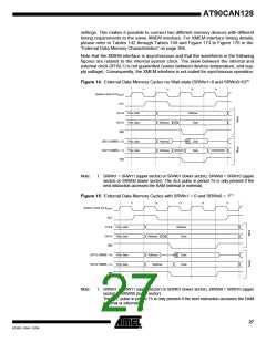
AT90CAN128
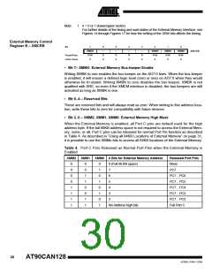
rides any pin direction settings in the respective data direction registers. Writing SRE to
zero, disables the External Memory Interface and the normal pin and data direction set-
tings are used. Note that when the XMEM interface is disabled, the address space
above the internal SRAM boundary is not mapped into the internal SRAM.
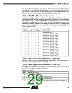
• Bit 6..4 – SRL2, SRL1, SRL0: Wait-state Sector Limit
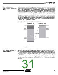
It is possible to configure different wait-states for different External Memory addresses.
The external memory address space can be divided in two sectors that have separate
wait-state bits. The SRL2, SRL1, and SRL0 bits select the split of the sectors, see Table
2 and Figure 12. By default, the SRL2, SRL1, and SRL0 bits are set to zero and the
entire external memory address space is treated as one sector. When the entire SRAM
address space is configured as one sector, the wait-states are configured by the
SRW11 and SRW10 bits.
Table 2. Sector limits with different settings of SRL2..0
SRL2
SRL1
SRL0
Sector Limits
Lower sector = N/A
Upper sector = 0x1100 - 0xFFFF
0
0
0
Lower sector = 0x1100 - 0x1FFF
Upper sector = 0x2000 - 0xFFFF
0
0
0
1
1
1
1
0
1
1
0
0
1
1
1
0
1
0
1
0
1
Lower sector = 0x1100 - 0x3FFF
Upper sector = 0x4000 - 0xFFFF
Lower sector = 0x1100 - 0x5FFF
Upper sector = 0x6000 - 0xFFFF
Lower sector = 0x1100 - 0x7FFF
Upper sector = 0x8000 - 0xFFFF
Lower sector = 0x1100 - 0x9FFF
Upper sector = 0xA000 - 0xFFFF
Lower sector = 0x1100 - 0xBFFF
Upper sector = 0xC000 - 0xFFFF
Lower sector = 0x1100 - 0xDFFF
Upper sector = 0xE000 - 0xFFFF
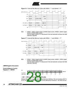
• Bit 3..2 – SRW11, SRW10: Wait-state Select Bits for Upper Sector
The SRW11 and SRW10 bits control the number of wait-states for the upper sector of
the external memory address space, see Table 3.
• Bit 1..0 – SRW01, SRW00: Wait-state Select Bits for Lower Sector
The SRW01 and SRW00 bits control the number of wait-states for the lower sector of
the external memory address space, see Table 3.
Table 3. Wait States(1)
SRWn1 SRWn0 Wait States
0
0
1
1
0
1
0
1
No wait-states
Wait one cycle during read/write strobe
Wait two cycles during read/write strobe
Wait two cycles during read/write and wait one cycle before driving out
new address
29
4250E–CAN–12/04

 ATMEL [ ATMEL ]