I/O Memory
The I/O space definition of the AT90CAN128 is shown in “Register Summary” on page
394.
All AT90CAN128 I/Os and peripherals are placed in the I/O space. All I/O locations may
be accessed by the LD/LDS/LDD and ST/STS/STD instructions, transferring data
between the 32 general purpose working registers and the I/O space. I/O registers
within the address range 0x00 - 0x1F are directly bit-accessible using the SBI and CBI
instructions. In these registers, the value of single bits can be checked by using the
SBIS and SBIC instructions. Refer to the instruction set section for more details. When
using the I/O specific commands IN and OUT, the I/O addresses 0x00 - 0x3F must be
used. When addressing I/O registers as data space using LD and ST instructions, 0x20
must be added to these addresses. The AT90CAN128 is a complex microcontroller with
more peripheral units than can be supported within the 64 location reserved in Opcode
for the IN and OUT instructions. For the Extended I/O space from 0x60 - 0xFF in SRAM,
only the ST/STS/STD and LD/LDS/LDD instructions can be used.
For compatibility with future devices, reserved bits should be written to zero if accessed.
Reserved I/O memory addresses should never be written.
Some of the status flags are cleared by writing a logical one to them. Note that, unlike
most other AVR’s, the CBI and SBI instructions will only operate on the specified bit, and
can therefore be used on registers containing such status flags. The CBI and SBI
instructions work with registers 0x00 to 0x1F only.
The I/O and peripherals control registers are explained in later sections.
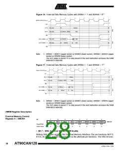
External Memory
Interface
With all the features the External Memory Interface provides, it is well suited to operate
as an interface to memory devices such as External SRAM and Flash, and peripherals
such as LCD-display, A/D, and D/A. The main features are:
•
•
Four different wait-state settings (including no wait-state).
Independent wait-state setting for different extErnal Memory sectors (configurable
sector size).
•
•
The number of bits dedicated to address high byte is selectable.
Bus keepers on data lines to minimize current consumption (optional).
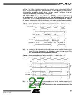
Overview
When the eXternal MEMory (XMEM) is enabled, address space outside the internal
SRAM becomes available using the dedicated External Memory pins (see Figure 2 on
page 4, Table 29 on page 69, Table 35 on page 73, and Table 47 on page 83). The
memory configuration is shown in Figure 12.
24
AT90CAN128
4250E–CAN–12/04

 ATMEL [ ATMEL ]