• Bit 6 – ICESn: Input Capture Edge Select
This bit selects which edge on the Input Capture pin (ICPn) that is used to trigger a cap-
ture event. When the ICESn bit is written to zero, a falling (negative) edge is used as
trigger, and when the ICESn bit is written to one, a rising (positive) edge will trigger the
capture.
When a capture is triggered according to the ICESn setting, the counter value is copied
into the Input Capture Register (ICRn). The event will also set the Input Capture Flag
(ICFn), and this can be used to cause an Input Capture Interrupt, if this interrupt is
enabled.
When the ICRn is used as TOP value (see description of the WGMn3:0 bits located in
the TCCRnA and the TCCRnB Register), the ICPn is disconnected and consequently
the Input Capture function is disabled.
• Bit 5 – Reserved Bit
This bit is reserved for future use. For ensuring compatibility with future devices, this bit
must be written to zero when TCCRnB is written.
• Bit 4:3 – WGMn3:2: Waveform Generation Mode
See TCCRnA Register description.
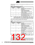
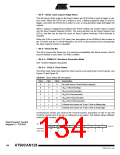
• Bit 2:0 – CSn2:0: Clock Select
The three Clock Select bits select the clock source to be used by the Timer/Counter, see
Figure 57 and Figure 58.
Table 64. Clock Select Bit Description
CSn2
CSn1
CSn0
Description
0
0
0
0
1
1
1
1
0
0
1
1
0
0
1
1
0
1
0
1
0
1
0
1
No clock source (Timer/Counter stopped).
clkI/O/1 (No prescaling)
clkI/O/8 (From prescaler)
clkI/O/64 (From prescaler)
clkI/O/256 (From prescaler)
clkI/O/1024 (From prescaler)
External clock source on Tn pin. Clock on falling edge.
External clock source on Tn pin. Clock on rising edge.
If external pin modes are used for the Timer/Countern, transitions on the Tn pin will
clock the counter even if the pin is configured as an output. This feature allows software
control of the counting.
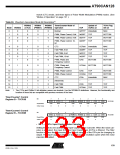
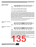
Timer/Counter1 Control
Register C – TCCR1C
Bit
7
FOC1A
R/W
0
6
FOC1B
R/W
0
5
FOC1C
R/W
0
4
–
3
–
2
–
1
–
0
–
TCCR1C
Read/Write
Initial Value
R
0
R
0
R
0
R
0
R
0
134
AT90CAN128
4250E–CAN–12/04

 ATMEL [ ATMEL ]