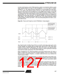
AT90CAN128
16-bit Timer/Counter
Register Description
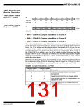
Timer/Counter1 Control
Register A – TCCR1A
Bit
7
6
5
4
3
2
1
0
COM1A1 COM1A0 COM1B1 COM1B0 COM1C1 COM1C0 WGM11
WGM10 TCCR1A
Read/Write
Initial Value
R/W
0
R/W
0
R/W
0
R/W
0
R/W
0
R/W
0
R/W
0
R/W
0
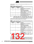
Timer/Counter3 Control
Register A – TCCR3A
Bit
7
6
5
4
3
2
1
0
COM3A1 COM3A0 COM3B1 COM3B0 COM3C1 COM3C0 WGM31
WGM30 TCCR3A
Read/Write
Initial Value
R/W
0
R/W
0
R/W
0
R/W
0
R/W
0
R/W
0
R/W
0
R/W
0
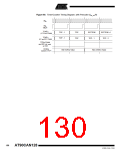
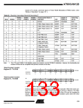
• Bit 7:6 – COMnA1:0: Compare Output Mode for Channel A
• Bit 5:4 – COMnB1:0: Compare Output Mode for Channel B
• Bit 3:2 – COMnC1:0: Compare Output Mode for Channel C
The COMnA1:0, COMnB1:0 and COMnC1:0 control the Output Compare pins (OCnA,
OCnB and OCnC respectively) behavior. If one or both of the COMnA1:0 bits are written
to one, the OCnA output overrides the normal port functionality of the I/O pin it is con-
nected to. If one or both of the COMnB1:0 bit are written to one, the OCnB output
overrides the normal port functionality of the I/O pin it is connected to. If one or both of
the COMnC1:0 bit are written to one, the OCnC output overrides the normal port func-
tionality of the I/O pin it is connected to. However, note that the Data Direction Register
(DDR) bit corresponding to the OCnA, OCnB or OCnC pin must be set in order to
enable the output driver.
When the OCnA, OCnB or OCnC is connected to the pin, the function of the COMnx1:0
bits is dependent of the WGMn3:0 bits setting. Table 60 shows the COMnx1:0 bit func-
tionality when the WGMn3:0 bits are set to a Normal or a CTC mode (non-PWM).
Table 60. Compare Output Mode, non-PWM
COMnA1/COMnB1/ COMnA0/COMnB0/
COMnC1
COMnC0
Description
0
0
Normal port operation, OCnA/OCnB/OCnC
disconnected.
0
1
1
0
Toggle OCnA/OCnB/OCnC on Compare Match.
Clear OCnA/OCnB/OCnC on Compare Match (Set
output to low level).
1
1
Set OCnA/OCnB/OCnC on Compare Match (Set
output to high level).
131
4250E–CAN–12/04

 ATMEL [ ATMEL ]